Supercharge Your Innovation With Domain-Expert AI Agents!

Manufacturing method of pixel structure and pixel structure

A pixel structure and manufacturing method technology, which is applied in semiconductor/solid-state device manufacturing, optics, instruments, etc., can solve the problems of affecting the electrical performance of the pixel structure, insufficient adhesion between the pixel electrode and the dielectric layer, and peeling off of the pixel electrode.

Inactive Publication Date: 2013-08-07
华映视讯(吴江)有限公司 +1
View PDF4 Cites 0 Cited by
  • Summary
  • Abstract
  • Description
  • Claims
  • Application Information

AI Technical Summary

Problems solved by technology

However, in this process, due to the difference in thermal expansion coefficient between the polycrystalline (poly-crystal) ITO film and the dielectric layer, the polycrystalline (poly-crystal) ITO film is prone to cracks during this high-temperature process ( crack)
In this way, the data voltage transmitted by the active component cannot be smoothly transmitted to the entire surface of the pixel electrode, so that the liquid crystal molecules above the crack of the pixel electrode cannot be normally deflected, resulting in abnormal display of the liquid crystal display
[0004] In order to prevent the problem that the polycrystalline indium tin oxide film is prone to cracks in the aforementioned high-temperature process, when the temperature of the high-temperature annealing process is lowered, the indium tin oxide film will affect the electrical performance of the pixel electrode due to insufficient crystallization. , It is also easy to make the adhesion between the pixel electrode and the dielectric layer insufficient, resulting in the pixel electrode being easily peeled off from the surface of the dielectric layer, which affects the overall electrical performance of the pixel structure

Method used


Image

  • Manufacturing method of pixel structure and pixel structure
  • Manufacturing method of pixel structure and pixel structure
  • Manufacturing method of pixel structure and pixel structure

Examples


Embodiment Construction

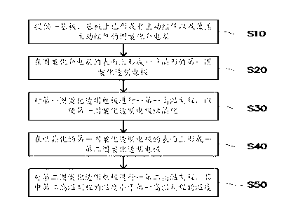
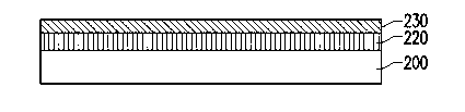
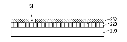
[0022] figure 1 It is a schematic flowchart of a manufacturing method of a pixel structure in a preferred embodiment of the present invention. Figure 2A to Figure 2F is a schematic cross-sectional view of a method for manufacturing a pixel structure in an embodiment of the present invention, and image 3 To take advantage of the aforementioned Figure 2A to Figure 2F An upper view of a pixel structure made by the method for making a pixel structure, wherein Figure 2F for correspondence image 3 Schematic cross-section along section line AA'.

[0023] Please refer to figure 1 , Figure 2A and image 3 , first provide a substrate 200, on which an active component 210 and a patterned dielectric layer 220 covering the active component 210 have been formed (step S10). The active component 210 is, for example, a thin film transistor, which includes a gate 212, a source 214 And the drain 216 , in this embodiment, the scanning line 218 is formed together during the process of...


PUM


Abstract

The invention discloses a manufacturing method of a pixel structure, and a pixel structure; the method comprises the following steps of: forming a driving component on a base plate; forming a patterned dielectric layer on the driving component; forming a first patterned transparent electrode on the surface of the patterned dielectric layer, and electrically connecting the first patterned transparent electrode with the driving component; performing a first high-temperature processing to the first patterned transparent electrode so as to crystallize the first patterned transparent electrode; forming a second patterned transparent electrode on the surface of the first patterned transparent electrode, wherein the pattern of the first patterned transparent electrode is substantially same as that of the second patterned transparent electrode; performing a second high-temperature processing to the second patterned transparent electrode, wherein the temperature of the second high-temperature processing is less than that of the first high-temperature processing; and in addition; the invention further discloses a pixel structure manufactured by using the manufacturing method.

Description

technical field [0001] The present invention relates to a method for manufacturing a pixel structure, and in particular to a method for manufacturing a pixel structure with a high-temperature process. Background technique [0002] A display is a communication interface between people and information, and flat-panel displays are currently the main development trend. There are mainly the following types of flat panel displays: organic electroluminescence display, plasma display panel, and liquid crystal display. Among them, liquid crystal displays are the most widely used. Generally speaking, a liquid crystal display is mainly composed of an active device array substrate, a color filter array substrate and a liquid crystal layer. Wherein, the active component array substrate includes a plurality of scan lines (scan lines), a plurality of data lines (data lines) and a plurality of pixel structures (pixel units) arranged in an array, and each pixel structure is respectively as...

Claims


Application Information

Patent Timeline
Patent Type & Authority Patents(China)
IPC IPC(8): H01L21/77G02F1/1343G02F1/1333H01L27/02
Inventor 蔡耀仁张锡明黄彦余
Owner 华映视讯(吴江)有限公司
Features
  • R&D
  • Intellectual Property
  • Life Sciences
  • Materials
  • Tech Scout
  • Unparalleled Data Quality
  • Higher Quality Content
  • 60% Fewer Hallucinations
Learn More