On-chip integrated inductor
A technology of integrating inductance and inductance coil, which is applied in the field of microelectronics, can solve the problems of large parasitic capacitance, reduce the quality factor Q of inductance and frequency bandwidth, etc., and achieve the effect of reducing parasitic capacitance, improving quality factor and expanding frequency bandwidth
- Summary
- Abstract
- Description
- Claims
- Application Information
AI Technical Summary
Problems solved by technology
Method used
Image

Examples
Embodiment 1
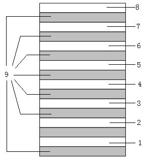
[0023] Such as figure 1 As shown, the on-chip integrated inductor of this embodiment has a one-to-eight-layer structure from bottom to top. The metal layers 1, 3, 5, and 7 are respectively arranged on the first, third, fifth, and seventh layers, and the inductance coils 2, 4, 6, and 8 are respectively arranged on the second, fourth, sixth, and eighth layers. An isolation layer 9 is provided between the two layers to realize electrical isolation between the upper and lower layers.
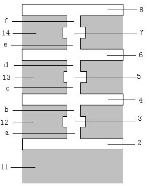
[0024] figure 2 for use figure 1 The structure diagram of the on-chip integrated inductor realized by the schematic diagram of the standard integrated circuit interconnection shown. figure 2 Among them, a layer of metal layers 3, 5, 7 and isolation layers 12, 13, 14 are arranged between two adjacent layers of inductance coils 2, 4, 6, 8. The inductance coils 2, 4, 6, 8 are connected to the metal layers 3, 5, 7 through the through holes a, b, c, d, e, f.
[0025] Wherein, the areas of the meta...
Embodiment 2
[0034] Figure 6 It is a cross-sectional view of the on-chip integrated inductor in this embodiment. In this embodiment, two metal layers are arranged between two adjacent layers of inductance coils, and the inductance coils 102, 105, 108 are located on the second layer, the fifth layer and the eighth layer. The inductance coil 108 is connected to the metal layer 107 through the perforation f, the metal layer 107 is connected to the metal layer 106 through the perforation e, the metal layer 106 is connected to the inductance coil 105 through the perforation d, the inductance coil 105 is connected to the metal layer 104 through the perforation c, and the metal layer 104 is connected to the metal layer 103 through the through hole b, and the metal layer 103 is connected to the inductance coil 102 through the through hole a. 16 to 28 are isolation layers, and 15 is a substrate.
[0035] Figure 7 It is a top view of the on-chip integrated inductor in this example, the inductan...
PUM
| Property | Measurement | Unit |
|---|---|---|
| Width | aaaaa | aaaaa |
| Width w | aaaaa | aaaaa |
Abstract
Description
Claims
Application Information
 - R&D
- Intellectual Property
- Life Sciences
- Materials
- Tech Scout
- Unparalleled Data Quality
- Higher Quality Content
- 60% Fewer Hallucinations
Browse by: Latest US Patents, China's latest patents, Technical Efficacy Thesaurus, Application Domain, Technology Topic, Popular Technical Reports.
© 2025 PatSnap. All rights reserved.Legal|Privacy policy|Modern Slavery Act Transparency Statement|Sitemap|About US| Contact US: help@patsnap.com