Preparation method of thin film transistor of flexible electronic device

A technology for flexible electronic devices and thin film transistors, which is applied in the field of solution manufacturing of thin film transistors of flexible electronic devices, can solve problems such as reduced structural reliability, structural voids, cracks, etc., so as to improve manufacturing efficiency, reduce production costs, and reduce The effect of key dimensions

Active Publication Date: 2011-08-31
WUHAN INTELLIGENT EQUIP IND INST CO LTD
View PDF2 Cites 25 Cited by
  • Summary
  • Abstract
  • Description
  • Claims
  • Application Information

AI Technical Summary

Problems solved by technology

Therefore, the existing inkjet printing technology is mostly used in the printing and manufacturing of PCB circuit boards, which cannot meet the requirements of high-resolution manufacturing of high-performance flexible electronics.
Invention patent CN 1425204A uses traditional inkjet printers to deposit materials on selected positions of the substrate. In the solution manufacturing of multiple transistors, the repulsion force of the second surface area to the selected solvent is greater than that of the first surface area, which is obtained by the user. Defined channel width, but minimum width is only 5 microns
[0006] (1) The resolution of the inkjet printing process is relatively low, usually 20-50 microns. Due to fa

Method used


Image

  • Preparation method of thin film transistor of flexible electronic device
  • Preparation method of thin film transistor of flexible electronic device
  • Preparation method of thin film transistor of flexible electronic device

Examples


Example Embodiment

[0048] Example 1

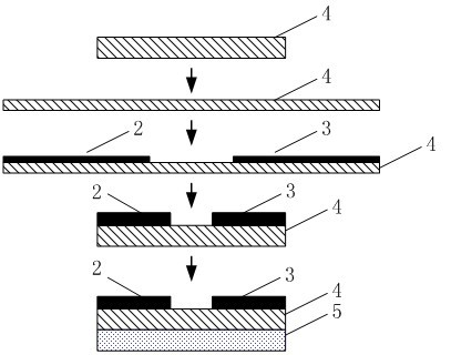
[0049] image 3 It is a schematic diagram of the process of preparing an all-organic thin film transistor (TFT) in Example 1 of the present invention. As can be seen from the figure, the process of preparing the present invention is:

[0050] (1) Prepare the substrate unit 4, which is a rubber substrate, which can be bent and stretched;

[0051] The flexible substrate selects a rubber substrate with high elastic deformation ability, which requires an elastic strain of more than 50%, and can be restored to its original state after the external force is released.

[0052] (2) Stretching and surface treatment for the substrate unit, usually stretching more than 50%, and coating the surface with adhesive;

[0053] In order to achieve the above purpose, the rubber substrate needs to have sufficient strength. The thickness of the rubber substrate can be referred to So that the rubber substrate can be restored to its original state as much as possible after releasing the ext...

Example Embodiment

[0064] Example 2

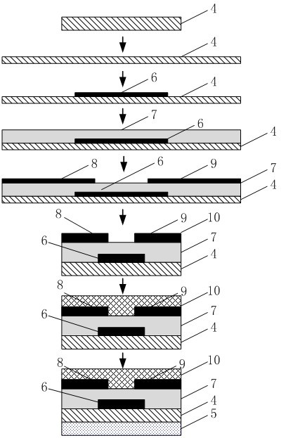
[0065] Figure 4 It is a schematic diagram of the process of manufacturing an organic-inorganic thin film transistor in Example 2 of the present invention. It can be seen from the figure that the process of manufacturing an organic-inorganic thin film transistor of the present invention is:

[0066] (1) Prepare the substrate unit 4, which is a rubber substrate, which can be bent and stretched;

[0067] The flexible substrate selects a rubber substrate with high elastic deformation ability, which requires an elastic strain of more than 50%, and can be restored to its original state after the external force is released.

[0068] (2) Stretching and surface treatment for the substrate unit, usually stretching more than 50%, and coating the surface with adhesive;

[0069] A layer of adhesive layer with a lower glass transition temperature is coated on the surface of the rubber substrate to realize the adhesion between the substrate and the functional layer. The glass tra...


PUM


Abstract

The invention provides a preparation method of a thin film transistor of a flexible electronic device. The method comprises the following steps of: (1) preparing a bendable and stretchable substrate; (2) stretching the substrate, and coating an adhesive on a surface of a stretched rubber substrate; (3) depositing a gate on the substrate; (4) depositing an organic dielectric layer unit on the device which is processed in the step (3); (5) respectively depositing a source unit layer and a drain unit layer on the organic dielectric layer unit; (6) loosening the substrate, releasing loads which are acted on the substrate, and carrying out heat treatment to eliminate an interface stress and a pressure stress of the device; and (7) depositing the organic dielectric layer unit. The invention provides the method for mechanically stretching the substrate, so the channel width of the device is reduced, manufacturing accuracy is improved effectively, and the resolution ratio of the flexible electronic device is improved.

Description

technical field [0001] The invention belongs to the technical field of flexible electronic device manufacturing, and in particular relates to a solution manufacturing method of a thin film transistor of a flexible electronic device. Background technique [0002] Electronic systems based on thin-film transistors (TFT) based on glass flat plates or flexible film bases are increasingly integrated in a large area, with a size of 1 meter or more, forming a so-called flexible electronic system. Its outstanding features are: low cost, light weight, thin shape , Good flexibility, in order to facilitate portability, these devices often need to be curled. However, conventional electronic devices are semiconductor chips formed from silicon wafers, which cannot be bent by themselves and are easily damaged during actual use. The use of large-area flexible thin films as substrates to construct organic or inorganic electronic devices is regarded as the driving force for the future develop...

Claims


Application Information

Patent Timeline
IPC IPC(8): H01L51/40
Inventor 黄永安尹周平陈建魁布宁斌王小梅段永青
Owner WUHAN INTELLIGENT EQUIP IND INST CO LTD
Why Eureka
Try Eureka