An OLED device and a manufacturing method thereof
A device and light-emitting layer technology, which is applied in the field of organic light-emitting diode devices, can solve the problems that the efficiency, color purity and color stability of red light OLED phosphorescent devices cannot be achieved simultaneously, and achieve the promotion of carrier balance, inhibition of exciton diffusion, The effect of improving the quality
- Summary
- Abstract
- Description
- Claims
- Application Information
AI Technical Summary
Problems solved by technology
Method used
Image
Examples
preparation example Construction
[0029] From the point of view of the preparation method of a kind of OLED device of the present invention: at first need prepare transparent conductive film 2 on substrate 1, etch OLED desired shape and clean; Then just can be in high vacuum (about 5 * 10 -4 Pa) for the preparation of multilayer structures. The preparation process is simple to see:
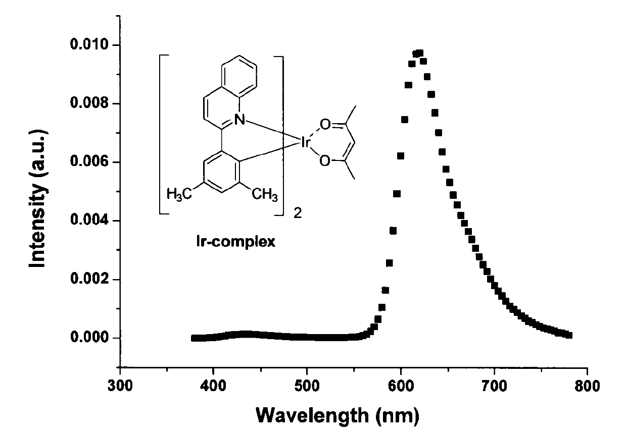
[0030]First, on the transparent conductive film 2, use a multi-source high-vacuum thermal deposition system to sequentially deposit the hole transport layer NPB on the cleaned and etched ITO surface, deposit a TAPC layer on the NPB layer, and use a double-source co-evaporation method on the TAPC layer. The method is to deposit TAPC:Ir-complexes, then sequentially double-source co-evaporation deposition of CBP:Ir-complexes and BCP:Ir-complexes, and then deposit a hole / exciton blocking layer on the light-emitting layer. Deposit a 3TPYMB or B3PyPPM layer on the barrier layer, then deposit a thin layer of LiF, and then deposit metal ...
Embodiment 1
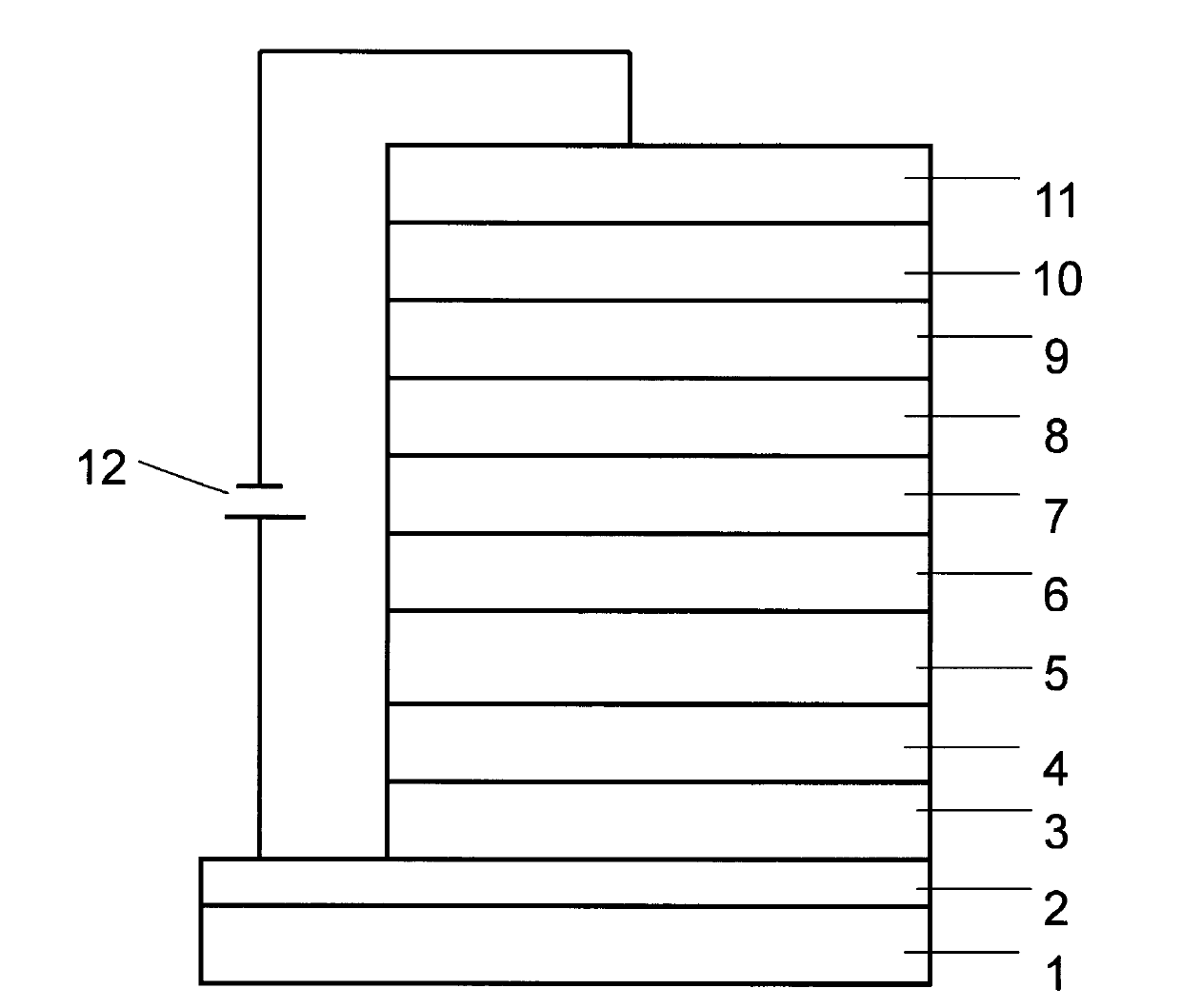
[0039] The substrate 1 is glass, and the transparent electrode 2 is an anode ITO film of 20 ohm / port. -4 Pa), deposit a hole transport layer 3 on the transparent electrode 2, that is, NPB with a thickness of 20nm, and then deposit a hole transport layer 4 on the hole transport layer 3, that is, a thickness of 5nm (thickness can be selected from 10nm, 15nm or 20nm, etc.) of TAPc; then deposit a light-emitting layer 6 on the hole-transport layer 4, and the light-emitting layer 6 evaporates CBP and Ir-complexes simultaneously by co-deposition, and the mass ratio of CBP and Ir-complexes is 100:X , where X is 5, 7, 9, 11, with different doping concentrations Ir-complex luminescent layer 6 with a thickness of 25nm; a hole-exciton blocking layer 8 is deposited on the luminescent layer 6, and the hole-exciton blocking The material of layer 8 is BCP, and the thickness is 20nm, 25nm or 30nm, etc.; after that, the electron injection layer 10 is deposited on the hole-exciton blocking laye...
Embodiment 2
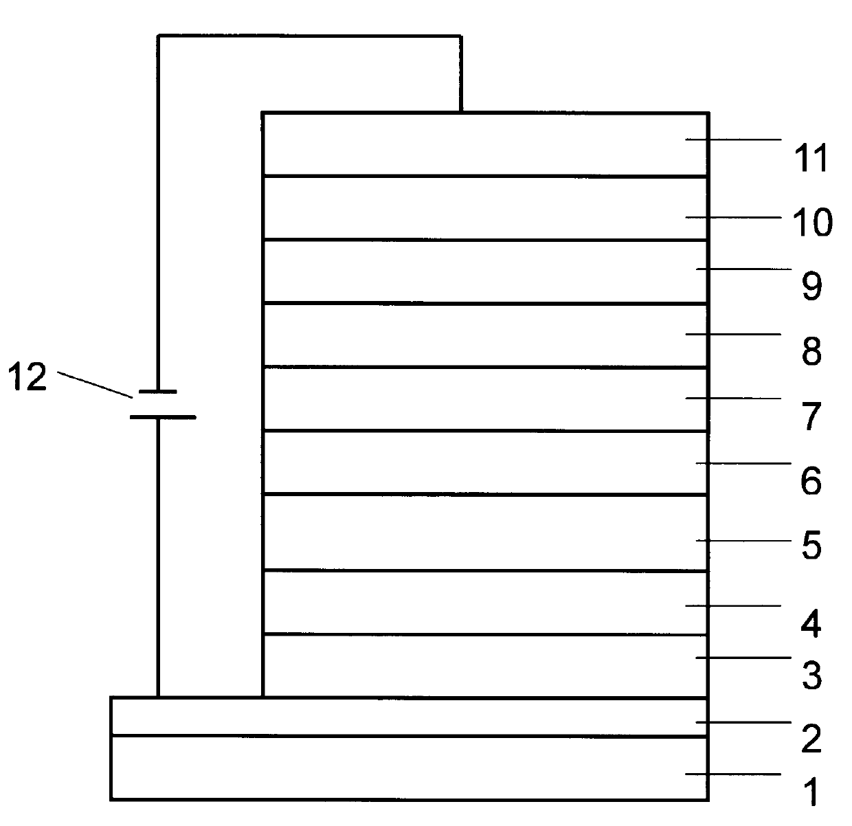
[0042] On the basis of Example 1, improve the light-emitting layer, increase the first doped light-emitting layer 5 of 8nm and the third doped light-emitting layer 7 of 8nm, the thickness of the second doped layer becomes 14nm, and the Ir-complex percentage of the doped layer Content is all 7%, and other preparation conditions are all identical with embodiment 1.
[0043] The test results of the packaged finished device show that the current density of the device with the addition of the first doped light-emitting layer and the third doped light-emitting layer is slightly reduced under the same voltage drive, the brightness is significantly increased, and the highest current efficiency reaches 13.7cd / A , the color purity CIE is (0.663, 0.334), and the maximum brightness of the device at 12V is 21860cd / m 2 .
PUM
| Property | Measurement | Unit |
|---|---|---|
| Thickness | aaaaa | aaaaa |
| Efficiency | aaaaa | aaaaa |
| Current efficiency | aaaaa | aaaaa |
Abstract
Description
Claims
Application Information


