Ta doped CeO2 depletion layer film and preparation method thereof

A transition layer and film technology, applied in the field of Ta-doped CeO2 transition layer film and its preparation, can solve the problems of hindering element diffusion and reaction, YBCO quality decline, film surface cracking, etc. textured effect

Inactive Publication Date: 2012-10-31
BEIJING UNIV OF TECH
View PDF0 Cites 2 Cited by
  • Summary
  • Abstract
  • Description
  • Claims
  • Application Information

AI Technical Summary

Problems solved by technology

But CeO 2 Due to its own nature, there is a certain critical film thickness when depositing on the base band, and exceeding this critical thickness will cause the film surface to crack and produce a large number of holes. This defect provides a short-range diffusion channel for the diffusion of oxygen, eventually leading to deposition YBCO's quality drops
At the same time, CeO 2 When the film is lower than this critical thickness, although good surface quality can be obtained, because the thickness is not enough, it also cannot hinder the diffusion and reaction of elements between the substrate and the YBCO superconducting layer.

Method used


Image

  • Ta doped CeO2 depletion layer film and preparation method thereof
  • Ta doped CeO2 depletion layer film and preparation method thereof
  • Ta doped CeO2 depletion layer film and preparation method thereof

Examples


Embodiment 1

[0026] 1) Dissolve cerium acetylacetonate and tantalum chloride in 4ml of n-propionic acid and 1ml of methanol, heat and stir until Completely dissolve to obtain the precursor solution;

[0027] 2) Apply the precursor solution to the cleaned NiW substrate by spin coating at a speed of 2000rpm for 30s to obtain a precursor film;

[0028] 3) in N 2 -H 2 (H 2 -4%) under gas protection atmosphere, heated to 950 ° C, took out after 5 minutes of heat preservation, and obtained a Ta with a thickness of 30 nm and a cubic texture. 0.1 Ce 0.9 o 2 Single transition layer film.

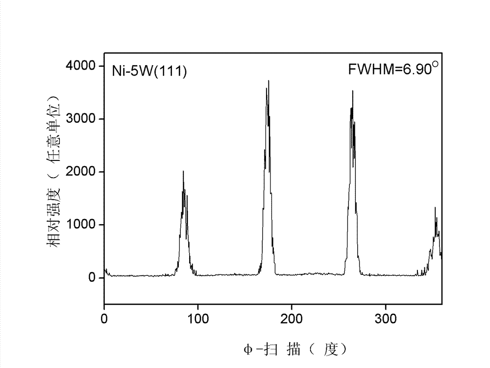
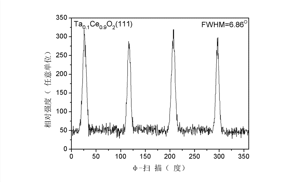
[0029] figure 1 It is the pole figure of the NiW metal substrate (111) used, showing that its in-plane height and width are 6.90; figure 2 For Ta 0.1 Ce 0.9 o 2 The (111) plane pole figure of the transition layer film has a FWHM (width at half maximum) of 6.86, which is lower than the in-plane FWHM value of the NiW baseband, proving that Ta 0.1 Ce 0.9 o 2 The transition layer film can not only impr...

Embodiment 2

[0031] 1) Dissolve cerium acetylacetonate and tantalum ethylate in 4ml of n-propionic acid at a molar ratio of cerium ions to tantalum ions of 4:1, with a total concentration of cerium ions and tantalum ions of 0.8mol / L, and heat and stir until completely dissolved to obtain Precursor;

[0032] 2) Apply the precursor solution to the cleaned NiW substrate by spin coating at a rotation speed of 5000rpm for 40s to obtain a precursor film;

[0033] 3) in N 2 -H 2 (H 2 -4%) under gas protection atmosphere, heat to 1200°C, take it out after 30 minutes of heat preservation,

[0034] 4) Obtain Ce with a thickness of 120nm and a cubic texture 0.67 Ta 0.33 o 2 Single transition layer film.

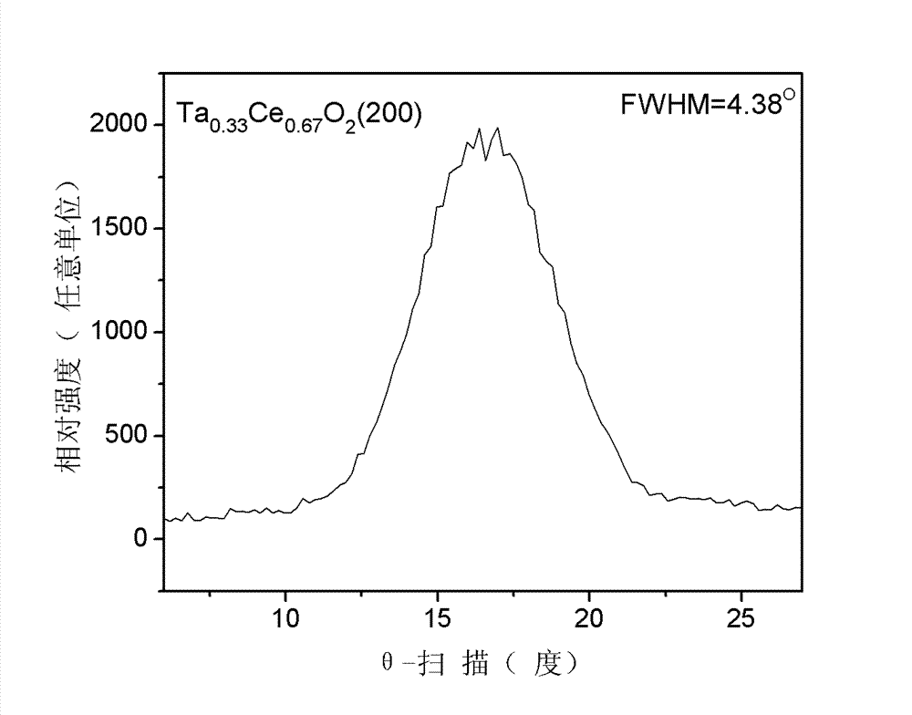
[0035] image 3 For Ta 0.2 Ce 0.8 o 2 The transition layer film has a rocking-curve of the out-of-plane half maximum value.

Embodiment 3

[0037] 1) Dissolve cerium acetylacetonate and tantalum ethylate in 4ml of n-propionic acid at a molar ratio of cerium ions to tantalum ions of 3:1, with a total concentration of cerium ions and tantalum ions of 0.4mol / L, and heat and stir until completely dissolved to obtain Precursor;

[0038] 2) Apply the precursor solution to the cleaned NiW base tape by spin coating, the rotation speed is 3000rpm, and the time is 60s to obtain the precursor film;

[0039] 3) in N 2 -H 2 (H 2 -4%) under gas protection atmosphere, heated to 1100°C, took it out after 60 minutes of heat preservation, and obtained a Ta with a thickness of 60nm and a cubic texture. 0.25 Ce 0.75 o 2 Single transition layer film.

[0040] Figure 4 For Ta 0.25 Ce 0.75 o 2 Depth-of-element analysis curve (AES) of a monolayer transition layer film. The sputtering speed is 10nm / min, and it can be obtained from the curve that the thickness of the single-layer film is 60nm.


PUM

PropertyMeasurementUnit
thicknessaaaaaaaaaa
thicknessaaaaaaaaaa
thicknessaaaaaaaaaa

Abstract

The invention discloses a Ta doped CeO2 depletion layer film and a preparation method thereof, belonging to the technical field of high-temperature coating superconducting materials. In the TaxCe1-xO2 film provided by the invention, the thickness of the depletion layer film is about 30-240nm. The preparation method comprises the following steps: dissolving Ta salt and Ce salt in methanol and propionic acid to obtain a precursor solution, wherein a cation molar ratio of Ta salt to Ce salt is x:(1-x), and x is larger than or equal to 0.1 and less than or equal to 0.25; then depositing the precursor solution on a Ni-5W base plate with a spin method; carrying out high temperature sintering in a protective atmosphere to obtain the TaxCe1-xO2 film. According to the invention, the preparation process is simple, cost is low, and the prepared film has the advantages of large thickness, good structure and less cracks and can isolate a superconducting layer to prevent it from reacting with a base material while extending texture.

Description

technical field [0001] The invention belongs to the technical field of high-temperature superconducting materials, in particular to a Ta-doped CeO 2 Transition layer film and its preparation method. Background technique [0002] CeO 2 Because of its minimum lattice mismatch with YBCO, good chemical stability at high temperature, and small thermal expansion coefficient, it has become the material of choice for the transition layer of the second-generation high-temperature coating superconductor, and has been extensively studied by researchers from all over the world. But CeO 2 Due to its own nature, there is a certain critical film thickness when depositing on the base band, and exceeding this critical thickness will cause the film surface to crack and produce a large number of holes. The quality of YBCO has dropped. At the same time, CeO 2 When the thin film is lower than this critical thickness, although good surface quality can be obtained, it cannot hinder the diffus...

Claims


Application Information

Patent Timeline
Patent Type & Authority Patents(China)
IPC IPC(8): C04B35/50C04B35/622
Inventor 刘敏吕昭索红莉马麟徐燕董传博
Owner BEIJING UNIV OF TECH
Why Eureka
Try Eureka