Method for manufacturing semiconductor device and method for manufacturing SiGe HBT (Heterojunction Bipolar Transistor)

A manufacturing method and semiconductor technology, which are applied in the manufacture of semiconductor/solid-state devices, electrical components, circuits, etc., can solve the problems that self-alignment of the base region and the emitter region cannot be well achieved, increase the cost of semiconductor devices, etc. Channel effect, reduce parasitic capacitance, raise the effect of source/drain region

Active Publication Date: 2011-09-14
SHANGHAI HUAHONG GRACE SEMICON MFG CORP
View PDF7 Cites 44 Cited by
  • Summary
  • Abstract
  • Description
  • Claims
  • Application Information

AI Technical Summary

Problems solved by technology

[0007] 1) In the prior art, when preparing a semiconductor device containing a CMOS transistor and a SiGe HBT transistor, it is necessary to sequentially manufacture a CMOS transistor and a SiGe HBT transis

Method used


Image

  • Method for manufacturing semiconductor device and method for manufacturing SiGe HBT (Heterojunction Bipolar Transistor)
  • Method for manufacturing semiconductor device and method for manufacturing SiGe HBT (Heterojunction Bipolar Transistor)
  • Method for manufacturing semiconductor device and method for manufacturing SiGe HBT (Heterojunction Bipolar Transistor)

Examples


Embodiment Construction

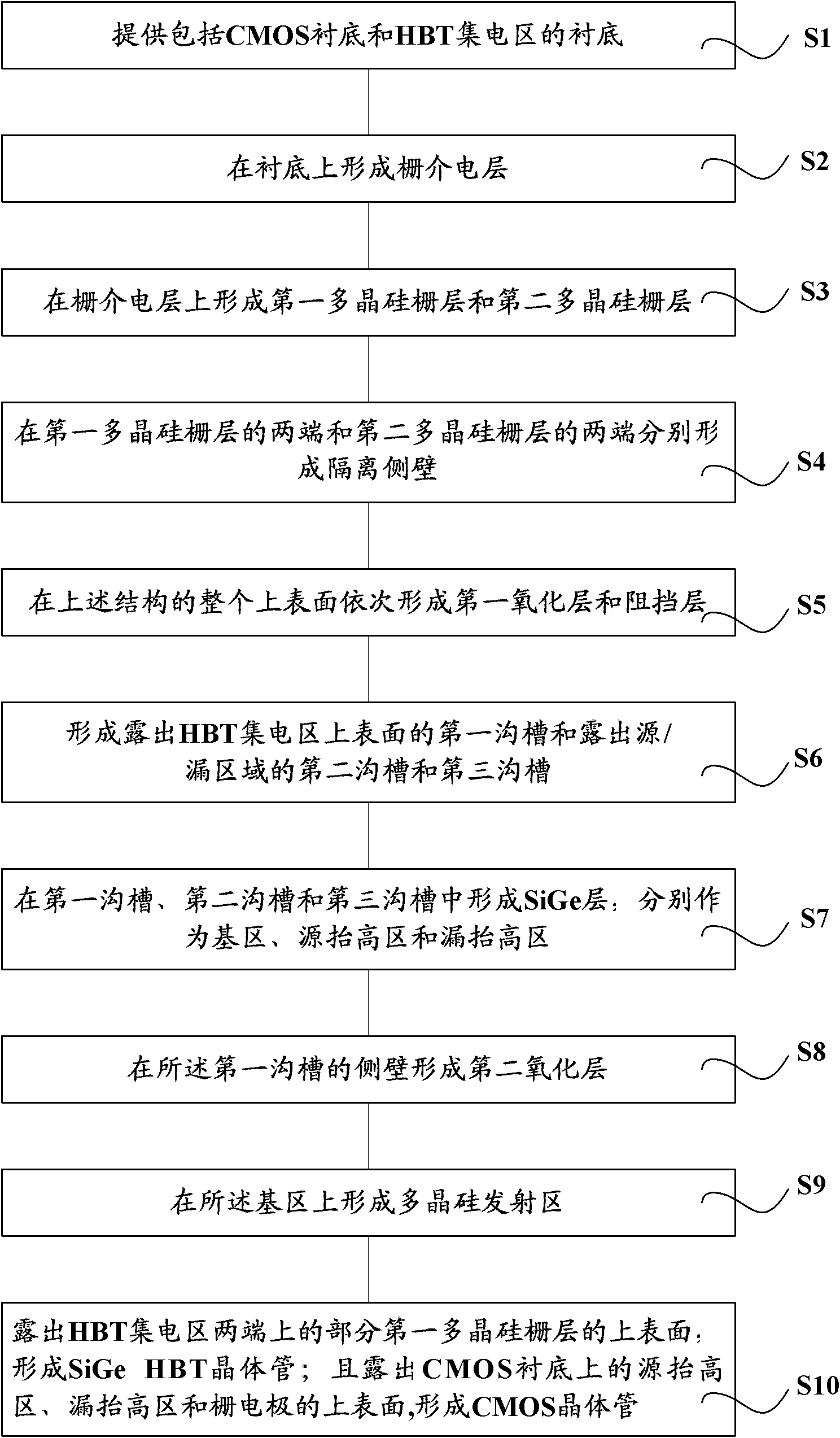
[0044] In order to make the above objects, features and advantages of the present invention more comprehensible, specific implementations of the present invention will be described in detail below in conjunction with the accompanying drawings.

[0045] In the following description, many specific details are set forth in order to fully understand the present invention, but the present invention can also be implemented in other ways than those described here, so the present invention is not limited by the specific embodiments disclosed below.

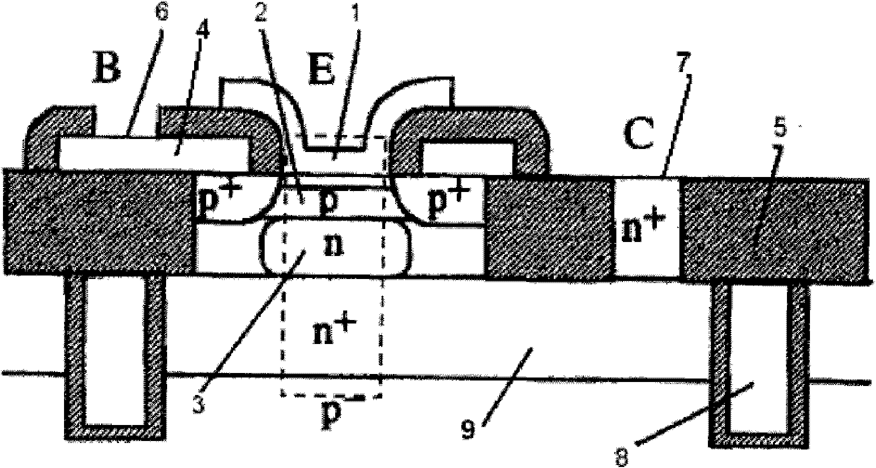
[0046] As mentioned in the background art, when fabricating semiconductor devices including SiGe HBT transistors and CMOS transistors in the prior art, there are disadvantages of high cost and the fact that the base region and the emitter region of the SiGe HBT transistor cannot be self-aligned.

[0047]In the present invention, the manufacturing process of the SiGe HBT transistor and the manufacturing process of the CMOS transistor are ef...


PUM


Abstract

The invention relates to a method for manufacturing a semiconductor device and a method for manufacturing an SiGe HBT (Heterojunction Bipolar Transistor), wherein the method for manufacturing the SiGe HBT comprises the steps of: offering a substrate comprising an HBT collector region; sequentially forming a gate dielectric layer, a polysilicon gate layer, an oxide layer and a barrier layer on the HBT collector region; removing partial barrier layer as well as the oxide layer, the polysilicon gate layer and the gate dielectric layer under the partial barrier layer on the HBT collector region so as to form a groove where the upper surface of the HBT collector region is exposed; forming an SiGe layer in the groove to serve as a base region; forming a polysilicon emitter region on the base region; and removing the partial barrier layer and the oxide layer under the partial barrier layer on two ends of the HBT collector region till the upper surface of partial polysilicon gate layer on the two ends of the HBT collector region is exposed and preserving the barrier layer surrounding the polysilicon emitter region and the oxide layer under the barrier layer. In the invention, the manufacturing processes of the two kinds of transistors are compatible and the cost is saved; the source/drain region of a CMOS (Complementary Metal Oxide Semiconductors) transistor is raised; and therefore, the self alignment of the base region and the emitter region of the SiGe HBT is realized.

Description

technical field [0001] The invention relates to the field of semiconductor technology, in particular to a method for manufacturing a semiconductor device and a method for manufacturing a SiGe (silicon germanium) HBT (Heterojunction Bipolar Transistor, heterojunction bipolar transistor) transistor. Background technique [0002] With the continuous development of microelectronics application technology, the performance of traditional silicon transistors is close to the theoretical limit. New types of transistors are being researched and developed as the basis for future microelectronics. Silicon germanium (SiGe) heterojunction bipolar transistors are one of them. SiGe heterojunction bipolar transistors are favored by the market for their low cost and high performance potential. [0003] The SiGe process is compatible with the Si device process and the BICMOS process, so it is more flexible in production. Under the same conditions, SiGe devices have higher frequency, faster ...

Claims


Application Information

Patent Timeline
IPC IPC(8): H01L21/8249H01L21/331
Inventor 孙涛陈乐乐
Owner SHANGHAI HUAHONG GRACE SEMICON MFG CORP
Why Eureka
Try Eureka