Preparation method of organic multilayer film
A multi-layer thin-film, organic technology, applied in semiconductor/solid-state device manufacturing, semiconductor devices, electrical components, etc., can solve problems affecting the luminous efficiency of organic materials, device performance, damage, etc., and achieve the effect of overcoming adverse effects and improving performance.
- Summary
- Abstract
- Description
- Claims
- Application Information
AI Technical Summary
Problems solved by technology
Method used
Image
Examples
Embodiment 1
[0015] The present invention proposes a kind of preparation method of organic multilayer thin film, comprises the steps:
[0016] Step 101: preparing metal electrodes on the two substrates by evaporation or sputtering;
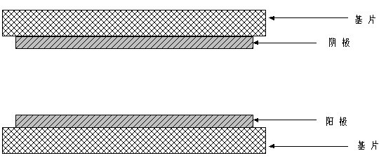
[0017] Such as figure 1 As shown, the metal anode or metal cathode electrode of the substrate is prepared by evaporation or sputtering, and the process flow is as follows: First, an indium tin oxide (ITO) metal anode is prepared on a substrate by evaporation or sputtering, with a thickness of 3500 angstroms, during the completion of the ITO evaporation process, the metal alignment mark of the anode electrode is made; then, on another substrate, the aluminum (Al) metal cathode electrode is also prepared by evaporation or sputtering, with a thickness of 4000 angstroms, and after the completion of the aluminum During the evaporation process, make the metal alignment mark of the cathode electrode;
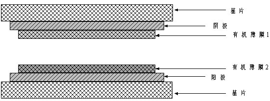
[0018] Step 102: Deposit different organic thin films on the me...
Embodiment 2
[0025] The difference between this embodiment and Embodiment 1 is that: Embodiment 1 heats two substrates, and this embodiment only heats one substrate. In this embodiment, the preparation of the substrate metal anode or metal cathode, the deposition of the metal anode or metal cathode organic thin film, and the alignment and contact of the substrate organic thin film are all the same as steps 101-103 in Embodiment 1. , which will not be described in detail in this embodiment. The differences between this embodiment and embodiment 1 are as follows:
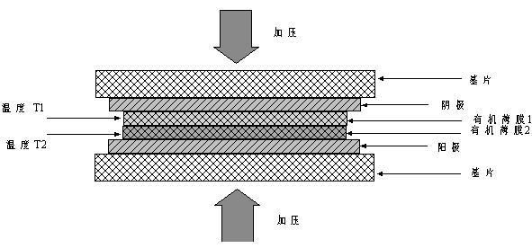
[0026] Step 104': heating one substrate, and applying pressure in opposite directions to the two substrates after the temperature of the substrate enters a preset temperature range;
[0027] The preset temperature range can be the glass transition temperature range of the organic thin film; in this embodiment, the metal anode substrate of indium tin oxide is not heated, only the aluminum metal cathode electrode substrate is heate...
PUM
 Abstract
Description
Claims
Application Information


