Semiconductor device and method for manufacturing same
A semiconductor and n-type technology, which is applied in semiconductor/solid-state device manufacturing, semiconductor devices, electrical components, etc., can solve problems such as increased channel resistance, decreased threshold voltage, and reduced withstand voltage, achieving low channel resistance and low channel resistance. The effect of channel resistance reduction
- Summary
- Abstract
- Description
- Claims
- Application Information
AI Technical Summary
Problems solved by technology
Method used
Image

Examples
no. 1 Embodiment approach
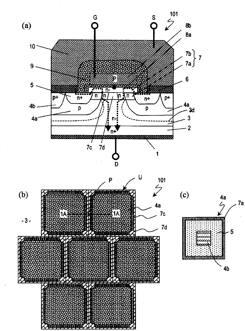
[0056] Hereinafter, a first embodiment of the semiconductor device of the present invention will be described. In this embodiment mode, a double injection type MOSFET will be described as an example. figure 1 (a) shows a cross-sectional structure of a part of the double injection type MOSFET 101, figure 1 (b) shows the planar structure of the drift layer 3 of the MOSFET101. figure 1 (a) means figure 1 In the cross-sectional structure of line 1A-1A in (b), MOSFET 101 includes a plurality of lattice units U. like figure 1 As shown in (b), on the drift layer 3 , each lattice unit U has, for example, a square shape, and the lattice units U are arranged in a zigzag shape. More specifically, the lattice units U are arranged two-dimensionally, and the arrangement of the lattice units U is shifted by 1 / 2 cycle in one direction. However, as will be described below, in MOSFET 101, the effect of the present invention can be obtained if lattice units U are arranged adjacent to e...
no. 2 Embodiment approach
[0110] Hereinafter, a second embodiment of the semiconductor device of the present invention will be described. Figure 7 (a) shows a cross-sectional structure of a part of the double injection type MOSFET 102, Figure 7 (b) shows a plan view of the drift layer 3 of the MOSFET 102 . Figure 7 (a) means Figure 7 The cross-sectional structure of line 6A-6A in (b). exist Figure 7 In (b), the structure of the cross-section shown by the line 1A-1A is the same as that of the first embodiment. Similar to the first embodiment, MOSFET 102 includes a plurality of lattice units U, and on drift layer 3, each lattice unit U has a square shape, and the square shape is arranged in a zigzag shape.
[0111] like Figure 7 As shown in (a) and (b), the difference between the MOSFET 102 and the first embodiment is that in the drift layer 3, it is adjacent to the fourth n-type impurity region 7d, and in the apex of the lattice unit U, There is also a fifth n-type impurity region 31 in plac...
experiment example
[0116] Hereinafter, in MOSFET 101 according to the first embodiment, experimental results regarding the effect on channel resistance when the impurity concentrations of the third n-type impurity region and the well are changed will be described.
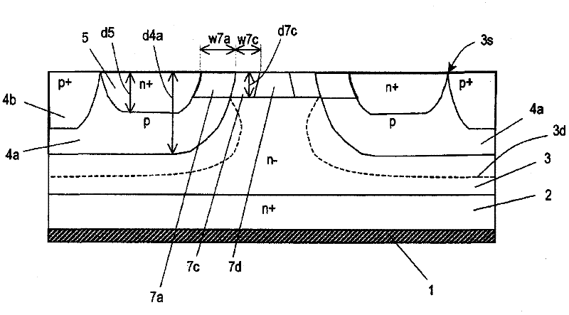
[0117] like Figure 7 As shown, the size of the lattice unit is set as Xcell, and the distance between the first n-type impurity regions 5 and the distance between the second n-type impurity regions 7a of two adjacent lattice units in the arrangement direction of the lattice units is The distances are set to a+2Lg and a respectively. The width of the second n-type impurity region 7a in the arrangement direction of the grid cells is represented by Lg which is the channel length. Table 1 shows the values used in the calculation.
[0118] (Table 1)
[0119]
[0120]
[0121] Figure 8 shows the channel resistance Rch when the carrier concentration Na of the first n-type impurity region 5 and the impurity concentration Next of ...
PUM
 Abstract
Description
Claims
Application Information
 - R&D
- Intellectual Property
- Life Sciences
- Materials
- Tech Scout
- Unparalleled Data Quality
- Higher Quality Content
- 60% Fewer Hallucinations
Browse by: Latest US Patents, China's latest patents, Technical Efficacy Thesaurus, Application Domain, Technology Topic, Popular Technical Reports.
© 2025 PatSnap. All rights reserved.Legal|Privacy policy|Modern Slavery Act Transparency Statement|Sitemap|About US| Contact US: help@patsnap.com