Power semiconductor device and method of manufacturing the same
A manufacturing method and semiconductor technology, applied in the fields of semiconductor/solid-state device manufacturing, semiconductor devices, electric solid-state devices, etc., can solve problems such as abnormal appearance inspection, current leakage, substrate damage, etc., to prevent the deterioration of process controllability, prevent Fluctuation of electrical characteristics, effect of avoiding damage
- Summary
- Abstract
- Description
- Claims
- Application Information
AI Technical Summary
Problems solved by technology
Method used
Image
Examples
Embodiment approach 1
[0029]
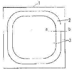
[0030] In the power semiconductor device of this embodiment, if figure 1 As shown, an annular trench 2 is formed in an end region along the edge of a chip (semiconductor substrate) 1 , and the inside of the trench 2 is defined as a cell region. Figure 15 yes means figure 1 A cross-sectional view showing the structure of the power semiconductor device according to the present embodiment in the a-b section.
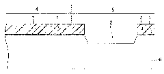
[0031] Such as Figure 15 As shown, the power semiconductor device of this embodiment has: an n-type silicon substrate 6; a trench 2 formed in the end region 5 of the silicon substrate 6; a p-type RESURF layer 9 formed at the lower part of the trench 2 The n-type channel stop layer 12 formed on the silicon substrate surface 3 outside the RESURF layer 9; the silicon oxide film 10 formed on the inner wall of the trench 2; the top of the silicon oxide film 10 is buried in the trench 2 Silicon oxide film 13 inside the trench 2; silicon oxide film 14 formed on the...
Embodiment approach 2
[0046]
[0047] In the manufacturing process of the power semiconductor device according to Embodiment 1, when the planarization process is performed by CMP, the surface of the silicon substrate 6 in the region where the trench 2 is not formed is covered with the silicon nitride film 7, so this becomes a barrier. layer, CMP is stopped, and the surface of the silicon substrate 6 is not ground. On the other hand, there is no silicon nitride film 7 in the trench 2 formed in the terminal region 5, but it is buried by the silicon oxide film 13. Therefore, when the planarization process is performed by CMP for a long time, until the surface of the silicon substrate 6 When the silicon nitride film 7 is completely exposed, the silicon oxide film 13 in the trench 2 is excessively polished and ground, and the thickness of the insulating film on the RESURF layer 9 becomes thin, possibly deteriorating the electrical characteristics.
[0048] In order to solve this problem, in the power ...
PUM
 Abstract
Description
Claims
Application Information


