III-nitride substrate growing method, substrate and LED (light emitting diode)

A growth method and nitride technology, applied in electrical components, circuits, semiconductor devices, etc., can solve the problems of complex growth process, graphene wrinkles, introduction of impurities, etc., and achieve the effect of simple growth process

Inactive Publication Date: 2011-09-28
SUZHOU NANOWIN SCI & TECH +1
View PDF2 Cites 35 Cited by
  • Summary
  • Abstract
  • Description
  • Claims
  • Application Information

AI Technical Summary

Problems solved by technology

[0005] The technical problem to be solved by the present invention is to provide a growth method of a III-nitride substrate and the substrate, and directly grow the III-nitride on the surface of graphene, which helps to overcome the complexity of the growth process and the wrinkle of graphene. and the introduction of impurities

Method used


Image

  • III-nitride substrate growing method, substrate and LED (light emitting diode)
  • III-nitride substrate growing method, substrate and LED (light emitting diode)
  • III-nitride substrate growing method, substrate and LED (light emitting diode)

Examples


Embodiment Construction

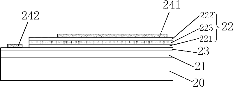
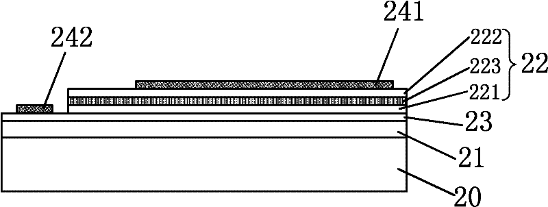
[0018] A method for growing a III-nitride substrate provided by the present invention and specific implementations of the substrate will be described in detail below with reference to the accompanying drawings.

[0019] The following uses the MOCVD process to grow GaN as an example for illustration. For materials such as AlN, InN and InGaN, except for a slight difference in the specific parameters of the growth process, the others are roughly the same as the following embodiments.

[0020] Preparation of graphene: chemical vapor deposition or graphite redox method can be used, preferably chemical vapor deposition. The specific implementation of the chemical vapor deposition method belongs to the known technology and will not be described in detail here.

[0021] Transfer of graphene: Spin-coat polydimethylsiloxane (PDMS) layer on graphene film, because PDMS has certain stickiness, can adhere to graphene film layer, and utilize chemical method to corrode graphene substrate, the...


PUM


Abstract

A III-nitride substrate growing method comprises the following steps: providing a copper support substrate; forming a graphene layer on the surface of the support substrate; and forming a III-nitride semiconductor layer on the surface of the graphene layer, wherein the highest growing temperature of the III-nitride semiconductor layer is lower than the melting point of copper. In the method, since graphene and III-nitride are sequentially grown on the conductive metallic copper substrate with high melting point, growth process is simple and impurities cannot be introduced in the production process.

Description

technical field [0001] The invention relates to the technical field of semiconductor devices and processes, in particular to a method for growing a Group III nitride substrate and the substrate. Background technique [0002] Gallium nitride, indium nitride, aluminum nitride and other group III nitrides and their ternary alloys, as the third-generation semiconductor materials, have been a research hotspot in the field of semiconductor materials in recent years, and have also been widely used in many aspects of production and life. fields. Group III nitrides and their alloys are all direct bandgap semiconductors, especially the alloy composed of three components can continuously control the bandgap width from 1.9eV to 6.2eV by adjusting the proportion of its components. In addition, the heterojunction structure made of group III nitrides and their alloys can form a two-dimensional electron gas with high concentration and high mobility, which makes up for the defects of large ...

Claims


Application Information

Patent Timeline
Patent Type & Authority Applications(China)
IPC IPC(8): H01L33/00H01L33/04
Inventor 徐耿钊王建峰刘争晖任国强蔡德敏钟海舰樊英民徐科
Owner SUZHOU NANOWIN SCI & TECH
Why Eureka
Try Eureka