

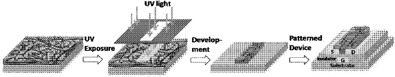
UV-lithographic micro-patterned organic thin film transistor semiconductor material and application
A technology of organic semiconductors and organic thin films, applied in the fields of semiconductor devices, semiconductor/solid-state device manufacturing, electric solid-state devices, etc., can solve the problems of photocrosslinkable semiconductor materials that have not been reported in any form.
- Summary
- Abstract
- Description
- Claims
- Application Information
AI Technical Summary
Problems solved by technology
Method used
Image

Examples
Embodiment 1
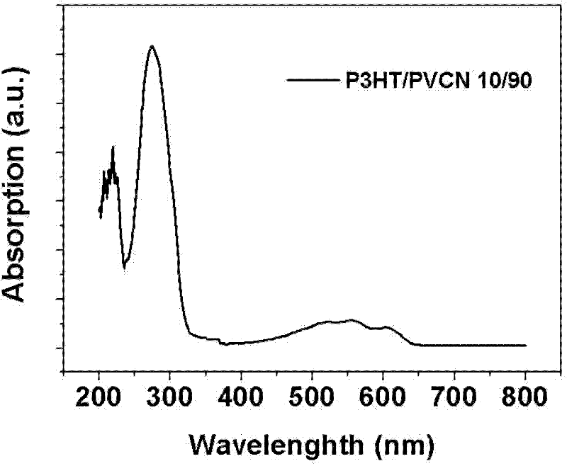
[0032] Dissolve P3HT and polyvinyl cinnamate (PVCN) in trichlorethylene at different ratios (P3HT / PVCN: 50% / 50%-1% / 99%) to make a solution with a concentration of 2%, and then To this solution was added dropwise 1-50 vol% dioxane; a thin film was prepared on a silicon wafer with a rotation speed of 2000 rpm.
Embodiment 2
[0034] Dissolve P3HT and polyvinyl cinnamate (PVCN) in different ratios (P3HT / PVCN: 50% / 50%-1% / 99%) in dichloromethane at 40°C to make a concentration of 2%. solution, and then the temperature of the solution was lowered to room temperature at a rate of 5°C / 10min, and a thin film was prepared on a silicon wafer with a rotation speed of 2000rpm.
Embodiment 3
[0036] Replace polyvinyl alcohol cinnamate with polyvinyl alcohol p-methyl cinnamate, and then prepare a film according to the steps in Example 2.
PUM
| Property | Measurement | Unit |
|---|---|---|
| Thickness | aaaaa | aaaaa |
Abstract
Description
Claims
Application Information