Manufacturing method of full back electrode solar cell

A technology for solar cells and manufacturing methods, which is applied in the manufacture of circuits, electrical components, and final products, and can solve problems such as high manufacturing costs and prices, difficult doping and diffusion control, and difficult alignment of graphics. Large-scale industrial production and application, good product uniformity, and high battery efficiency

Inactive Publication Date: 2011-10-05
徐荣
View PDF5 Cites 15 Cited by
  • Summary
  • Abstract
  • Description
  • Claims
  • Application Information

AI Technical Summary

Problems solved by technology

However, during the subsequent high-temperature diffusion of the dopant source printed on the back of the solar cell, the phosphorus-rich gas in the furnace will not only diffuse to the front of the solar cell, but also affect the dopant printed on the back of the solar cell. The influence of the source makes it difficult to control the doping diffusion on the back side accurately, thus affecting the uneven quality of the final solar cell, which is v

Method used


Image

  • Manufacturing method of full back electrode solar cell
  • Manufacturing method of full back electrode solar cell
  • Manufacturing method of full back electrode solar cell

Examples


Embodiment Construction

[0030] In order to have a clearer understanding of the technical features, purposes and effects of the present invention, the specific implementation manners of the present invention will now be described with reference to the accompanying drawings. Wherein, the same parts adopt the same reference numerals.

[0031] Based on the description of the relevant prior art in the background art, in the following embodiments of the present invention, the structure and principle of the all-back electrode solar cell will not be described in detail to save space.

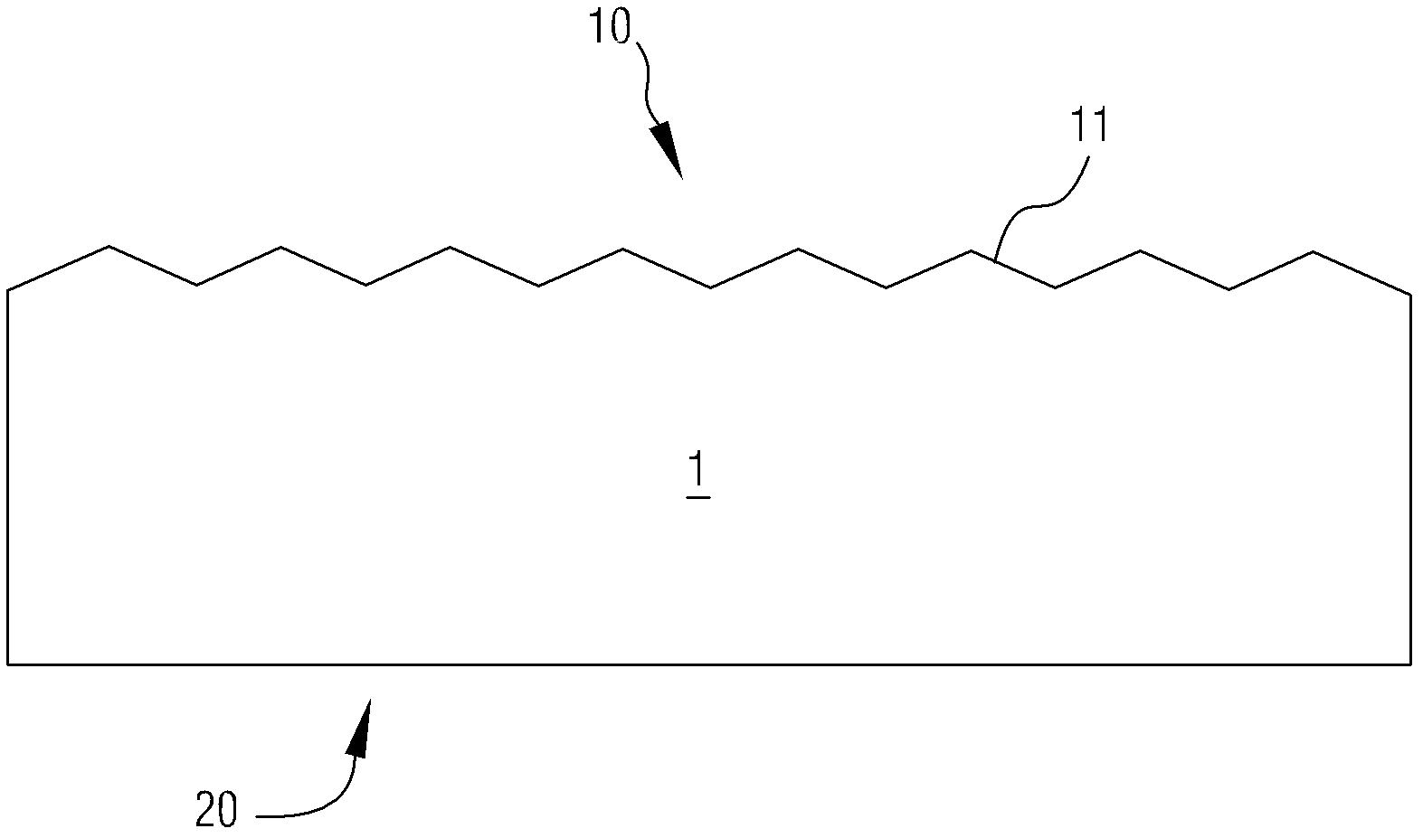
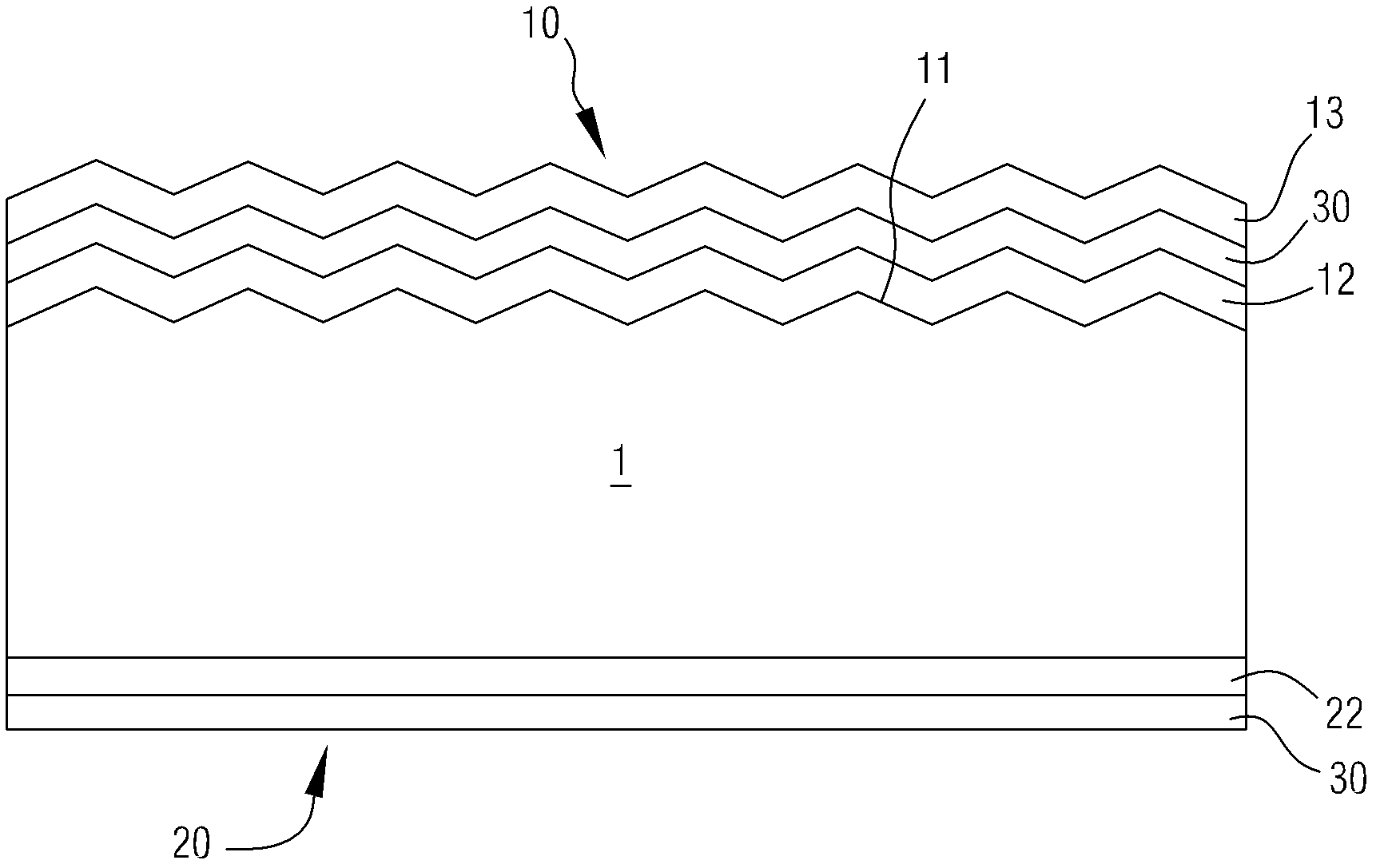
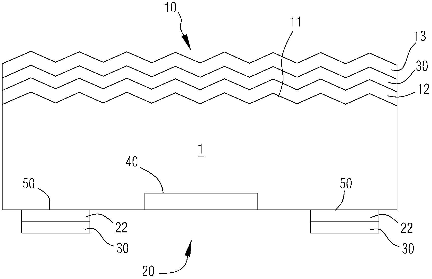
[0032] According to a specific embodiment of the present invention, a method for making a full-back electrode solar cell can refer to Figure 1-5 The process flow is described in detail, as shown in the figure, in the manufacturing method of the full back electrode solar cell of the present invention, the solar cell includes a silicon wafer 1, in this embodiment, the silicon wafer 1 is an N-type silicon wafer, The silicon chi...


PUM


Abstract

The invention relates to a manufacturing method of a full back electrode solar cell. According to the invention, after a damaged layer of a silicon chip is removed and a texturing process is carried out on a right side of the silicon chip, a phosphorus diffusion process is carried out on the silicon chip, and a right side filed and a back side field are formed. Oxide films are respectively formedon the right side and the back side of the silicon chip. And then, a part of the oxide film and a part of the back side field at the back of the silicon chip are removed, wherein the part of the oxide film and the part of the back side field are at a place where an electrode of an emitter electrode is needed to be formed; and meanwhile, another part of oxide film and another part of back side field are kept, wherein the another part of oxide film and the another part of back side field are at a place where a base electrode is needed to be formed. At last, by using the kept oxide film as a mask, a diffusion process is carried out on the back side of the silicon chip, wherein the processed area is where the oxide film and the back side field have been removed, so that the emitter electrode is formed. The full back electrode solar cell, which is produced by the method provided in the invention, has advantages of simple technology and high cell efficiency; besides, the assembly of the solar cell is easy to be welded. In addition, because the technology employed by the invention does not require especially-designed equipment, the cost is low, and produced production has good homogenization. Therefore, the manufacturing method of the full back electrode solar cell is suitable for large-scale industrialization production and application.

Description

technical field [0001] The invention relates to a method for manufacturing a solar cell, in particular to a method for manufacturing a full-back electrode solar cell, and belongs to the field of solar cell manufacturing. Background technique [0002] A solar cell is a semiconductor component that converts sunlight into electricity, so the efficiency of a solar cell is closely related to the light absorption of the solar surface. [0003] In the manufacturing process of crystalline silicon solar cells, there are often many metal grid lines on the light-receiving surface of the solar cells obtained in the conventional manufacturing process, and the purpose is to collect current and serve as soldering points of components. On the one hand, the existence of the metal grid lines blocks the absorption of sunlight and reduces the conversion efficiency of the battery. On the other hand, during the production process of the module, because the positive and negative electrode pads are...

Claims


Application Information

Patent Timeline
IPC IPC(8): H01L31/18
CPCY02P70/50
Inventor 杨华
Owner 徐荣
Why Eureka
Try Eureka