Piezoelectric element and preparation method thereof

A piezoelectric element and piezoelectric technology, applied in the field of piezoelectric elements and their preparation, can solve the problems of easy brittleness, poor reliability of piezoelectric elements, and poor elasticity of piezoelectric ceramic nanowires, and achieve excellent elasticity. , the effect of excellent elasticity and piezoelectric properties

Inactive Publication Date: 2011-10-05
徐文光
View PDF6 Cites 4 Cited by
  • Summary
  • Abstract
  • Description
  • Claims
  • Application Information

AI Technical Summary

Problems solved by technology

[0004] However, the piezoelectric element made by using piezoelectric ceramic nanowires can only generate a current of about 10 -12 -10 -9 Ampere or so, and because the piezoelectric ceramic nanowire itself has poor elasticity and is easy to be brittle, it often leads to poor reliability of the piezoelectric element produced
Therefore, there is an urgent need in the art for a piezoelectric element with a novel structure, which can improve the shortcomings of existing piezoelectric elements such as low current and piezoelectric ceramic nanowires that are easily brittle and cause poor reliability, and increase the piezoelectric element. Reliability and scope of application

Method used


Image

  • Piezoelectric element and preparation method thereof
  • Piezoelectric element and preparation method thereof
  • Piezoelectric element and preparation method thereof

Examples


Embodiment 1

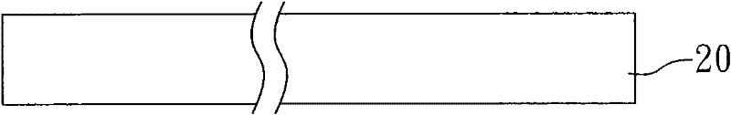
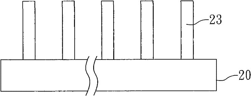
[0057] see Figure 2A-Figure 2H , which is a schematic diagram of the fabrication process of the piezoelectric element of this embodiment. First, (a) provide a substrate 20 (such as Figure 2A shown); then (b) forming a plurality of carbon nanotubes 23 on the surface of the substrate 20 (such as Figure 2B shown). In this embodiment, the substrate 20 used is a silicon-based substrate.

[0058] And then, (c) form a zinc oxide layer 24 (that is, a piezoelectric ceramic layer) on the surface of a plurality of carbon nanotubes 23 (such as Figure 2C shown). Here, the zinc oxide layer 24 is formed on the surfaces of the plurality of carbon nanotubes 23 by atomic layer deposition. And, (c0) repeat the step 800 times (not shown) of forming the zinc oxide layer 24 on the surface of the plurality of carbon nanotubes 23 in the step (c), so that the total thickness of the zinc oxide layer 24 reaches a predetermined value (about ).

[0059] Then, (d) use a thermal vaporization met...

Embodiment 2

[0068] see Figure 4A-Figure 4F , which is the flow chart of the preparation of the piezoelectric element of this embodiment. First, (a) provide a substrate 20 (such as Figure 4A shown); then (b) forming a plurality of carbon nanotubes 23 on the surface of the substrate 20 (such as Figure 4B shown). In this embodiment, the substrate 20 used is a silicon-based substrate.

[0069] And then, (c) form a zinc oxide layer 24 on the surface of a plurality of carbon nanotubes 23 (such as Figure 4C shown). Here, the zinc oxide layer 24 is formed on the surface of the plurality of carbon nanotubes 23 by atomic layer deposition. And, (c0) repeat the step 800 times (not shown) of forming the zinc oxide layer 24 on the surface of the plurality of carbon nanotubes 23 in the step (c), so that the total thickness of the zinc oxide layer 24 reaches a predetermined value (about ).

[0070] Then, (d) use a vacuum infiltration method to fill a supporting material 25 between a plurality...

Embodiment 3

[0074] A piezoelectric block 3 is prepared in the same manner as in Example 2 (steps (a) to (e) of Example 3), such as Figure 4A to Figure 4F shown. Next, if Figure 5 As shown, proceed to step (f1): respectively form the first conductive layer 21 and the second conductive layer 22 on the two side surfaces 33, 34 of the piezoelectric block 3, and make the first conductive layer 21 and the second conductive layer 22 respectively It is electrically coupled with the zinc oxide layer 24 in the piezoelectric block 3 .

[0075] like Figure 5 As shown, in the piezoelectric element 2 of this embodiment, the first conductive layer 21 and the second conductive layer 22 are connected in series with the piezoelectric block 3 (that is, the first conductive layer 21 and the second conductive layer 22 The surface of the piezoelectric block 3 is roughly parallel to the arrangement direction of the carbon nanotubes 23 in the piezoelectric block 3). And when the series length L2 exceeds 2...


PUM


Abstract

The invention relates to a piezoelectric element and a preparation method thereof. The piezoelectric element comprises multiple nano carbon tubes, piezoelectric ceramic layers and a support material, wherein the piezoelectric ceramic layers are coated on the surfaces of the nano carbon tubes and the support material is configured among the multiple nano carbon tubes the surfaces of which are coated with the piezoelectric ceramic layers so as to support the nano carbon tubes; the multiple nano carbon tubes are ranked in a comb shape; the piezoelectric ceramic layers configured on the surfaces of the multiple piezoelectric ceramic layers are electrically coupled mutually; and the multiple nano carbon tubes, at least one piezoelectric ceramic layer and the support material constitute a piezoelectric block. The piezoelectric element has good elasticity (durability) and good piezoelectric property, and when the size of the piezoelectric element is 2.5mm*1mm*1mm (length*width*height), the measured current reaches about 1.5mu A, and the voltage reaches above 1 V.

Description

technical field [0001] The invention relates to a piezoelectric element and a preparation method thereof, in particular to a piezoelectric element and a preparation method thereof using nanometer carbon tubes covered with a piezoelectric ceramic layer as a piezoelectric material. Background technique [0002] Piezoelectric effect is a phenomenon in which mechanical energy and electrical energy are exchanged in materials, and piezoelectric materials have piezoelectric effect because of the special arrangement of atoms in the crystal lattice, which makes the material have the effect of coupling stress field and electric field. Piezoelectric materials are used in a wide range of applications, such as: biochemical medical applications, wind or tidal power generation devices, wireless sensors, personal electronics, etc. Common piezoelectric materials include ceramic barium titanate (BaTiO 3 , BT), lead zirconium titanate (Pb(Zr 0.53 Ti 0.47 )O 3 , PZT), single crystal quartz ...

Claims


Application Information

Patent Timeline
Patent Type & Authority Applications(China)
IPC IPC(8): H01L41/113H01L41/16H01L41/22H01L41/293
Inventor 徐文光郭信甫林育贤唐炯文吕杰琏赖耀成
Owner 徐文光
Why Eureka
Try Eureka