Semiconductor structure and manufacturing method thereof

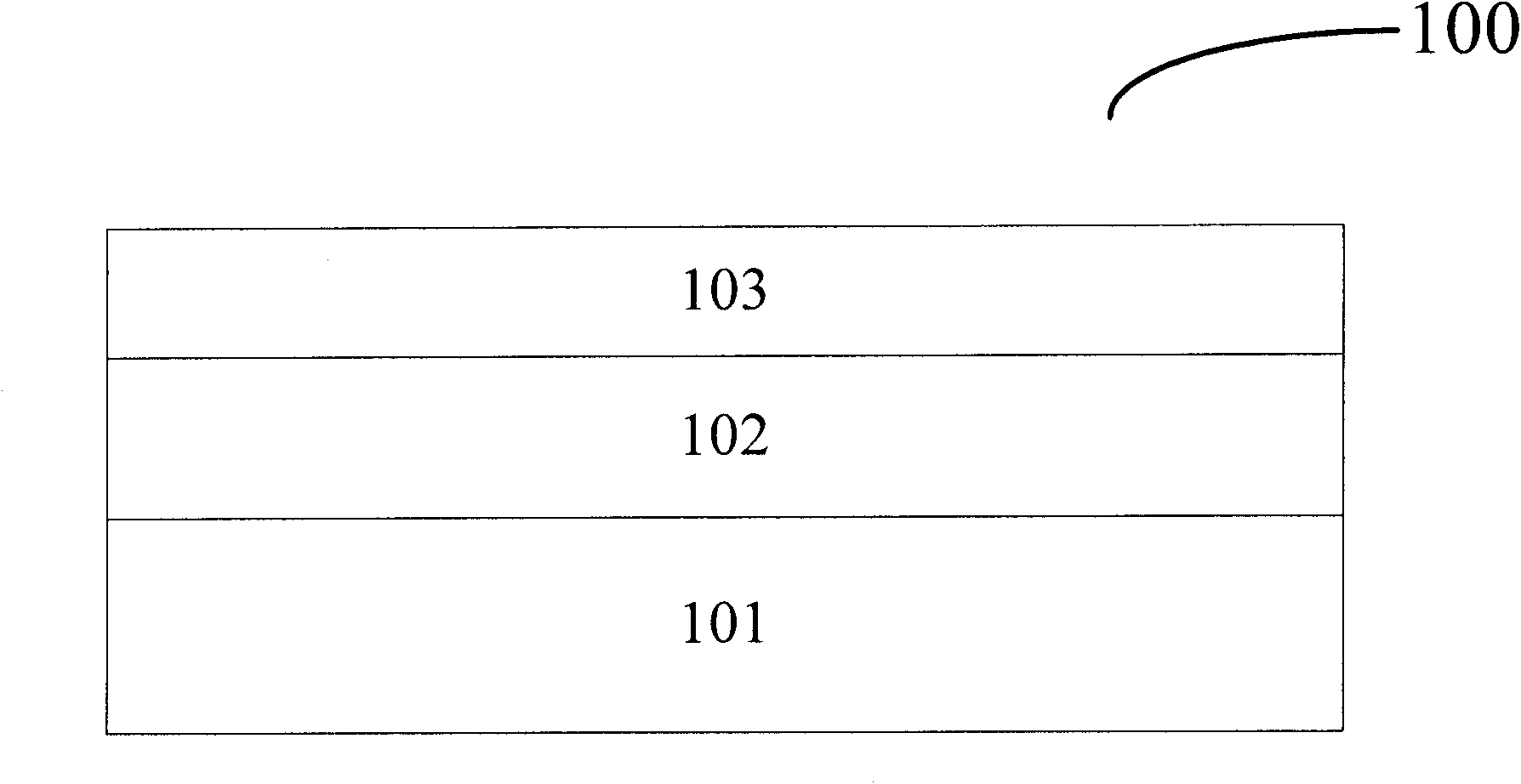
A semiconductor and wide bandgap technology, which is applied in the field of semiconductor structure and its manufacturing, can solve the problems of poor uniformity of the top layer silicon 103, difficult to control the thickness, and low yield rate, etc., and achieve the goal of suppressing the short channel effect and improving the electrical and physical properties Effect

Inactive Publication Date: 2011-10-12
INST OF MICROELECTRONICS CHINESE ACAD OF SCI
View PDF5 Cites 0 Cited by
  • Summary
  • Abstract
  • Description
  • Claims
  • Application Information

AI Technical Summary

Problems solved by technology

The manufacture of ultra-thin silicon-on-insulator by wafer bonding technology requires high process requirements, and it is easy to cause lattice defects on the contact surface during wafer bonding, resulting in low yield
In addition, because it is difficult to control the thickness of the ultra-thin silicon layer, the uniformity of the top layer silicon 103 on the buried oxide layer is poor

Method used


Image

  • Semiconductor structure and manufacturing method thereof
  • Semiconductor structure and manufacturing method thereof
  • Semiconductor structure and manufacturing method thereof

Examples


Embodiment Construction

[0019] The semiconductor structure and the manufacturing method thereof provided by the embodiments of the present invention solve the problems of high ultra-thin silicon-on-insulator process requirements and low yield, and better suppress the short channel effect.

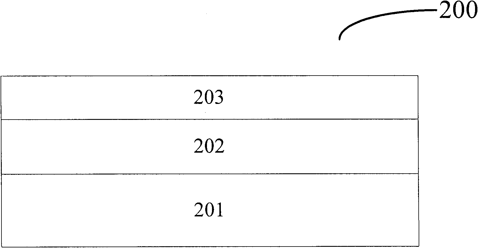
[0020] figure 2 A schematic structural diagram of a semiconductor structure 200 according to an embodiment of the present invention is shown. Such as figure 2 As shown, the semiconductor structure 200 includes a silicon substrate 201 , one or more wide bandgap semiconductor layers 202 formed on the silicon substrate, and a silicon layer 203 formed on the one or more wide bandgap semiconductor layers 202 . Wherein, the thickness of one or more wide bandgap semiconductor layers 202 is preferably 5-50 nm, and the thickness of the silicon layer 203 is preferably 5-20 nm. The top silicon layer 203 may also be referred to as top silicon.

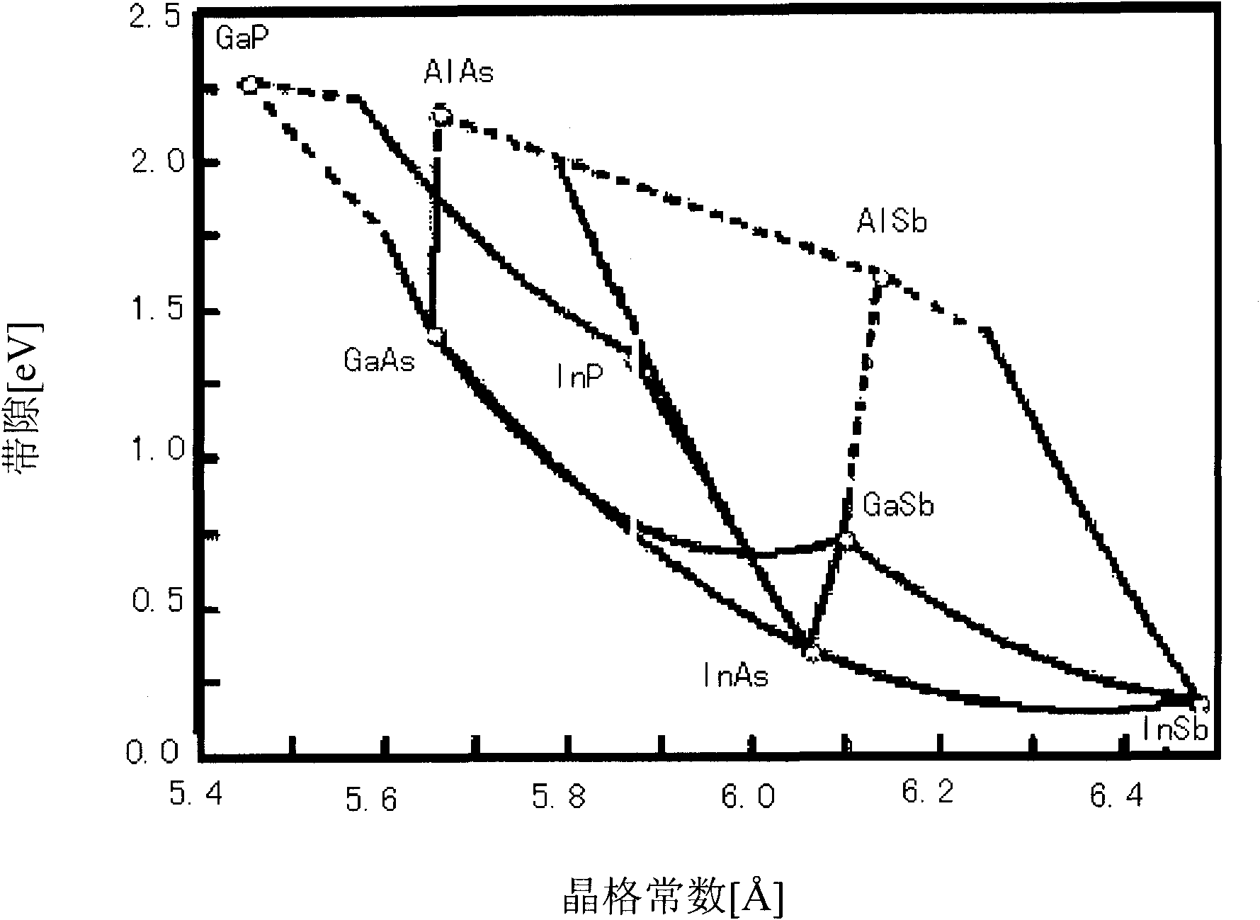
[0021] image 3 The relationship between the band gap and the lattice const...


PUM


Abstract

The invention provides a semiconductor structure and a manufacturing method thereof, relating to the field of semiconductor manufacturing. The semiconductor structure comprises a silicon substrate, a wide band gap semiconductor layer formed on the silicon substrate and a silicon layer formed on the wide band gap semiconductor layer. The method comprises the steps of growing the wide band gap semiconductor layer on the silicon substrate and growing the silicon layer on the wide band gap semiconductor layer. The embodiment of the invention can be applied to manufacturing of semiconductor devices.

Description

technical field [0001] The invention relates to semiconductor manufacturing technology, in particular to a semiconductor structure and a manufacturing method thereof. Background technique [0002] A general trend in modern integrated circuit fabrication is to produce semiconductor devices, such as memory cells, of ever smaller dimensions. [0003] Although fabrication of transistors at the nanometer scale allows the integration of more transistors on a single wafer, thereby enabling the formation of larger circuitry in a smaller area, the continuous shrinking of transistor dimensions leads to a decrease in channel length, causing increasingly Severe short channel effect (SCE) occurs. [0004] Ultra-thin silicon-on-insulator (UTSOI) is a typical technology for suppressing short-channel effects. Such as figure 1 As shown, in the silicon-on-insulator structure 100, there is a layer of silicon dioxide 102 as an insulating layer between the silicon substrate 101 and the top la...

Claims


Application Information

Patent Timeline
Patent Type & Authority Applications(China)
IPC IPC(8): H01L21/20
CPCH01L21/02381H01L21/02461H01L21/02463H01L21/02532H01L21/02439
Inventor 尹海洲朱慧珑骆志炯
Owner INST OF MICROELECTRONICS CHINESE ACAD OF SCI
Why Eureka
Try Eureka