

Polysilicon nanowire solar cell and preparation method thereof
A technology of solar cells and nanowires, applied in circuits, photovoltaic power generation, electrical components, etc., can solve the problems of high cost of preparation methods, achieve strong anti-reflection properties, enhance absorption, and increase collection effects
- Summary
- Abstract
- Description
- Claims
- Application Information
AI Technical Summary
Problems solved by technology
Method used
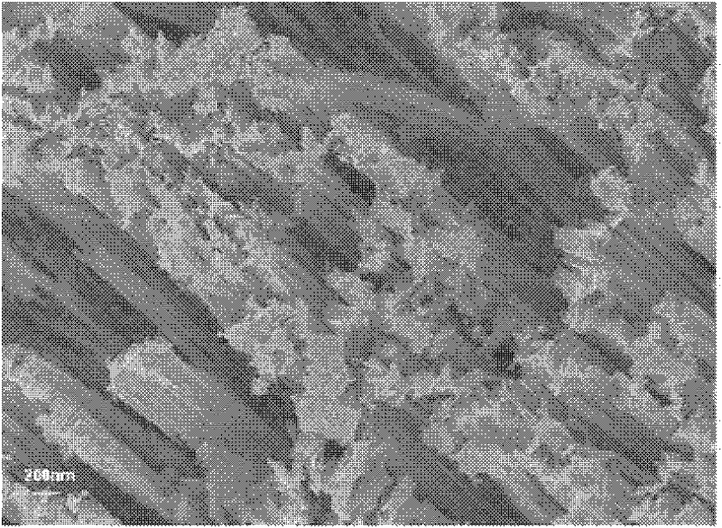
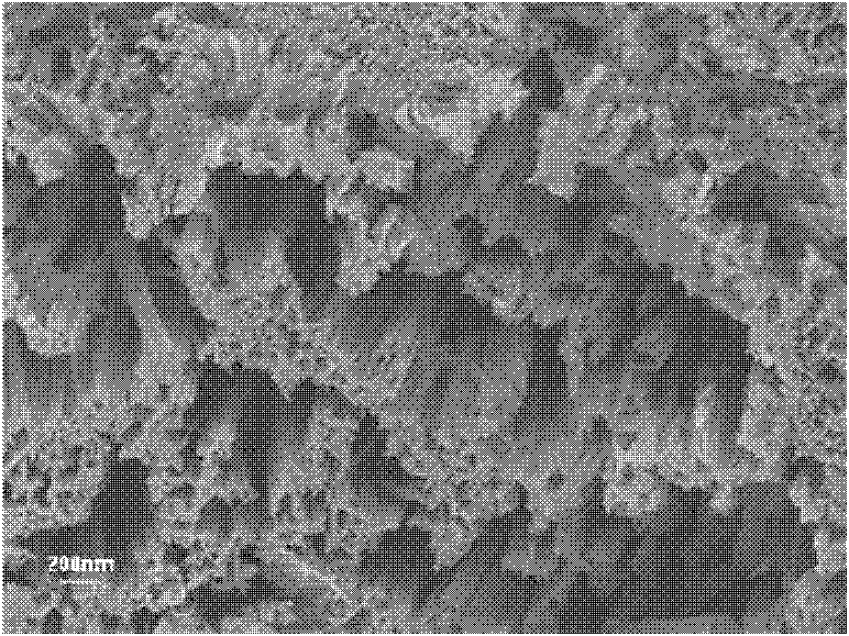
Image

Examples
Embodiment 1
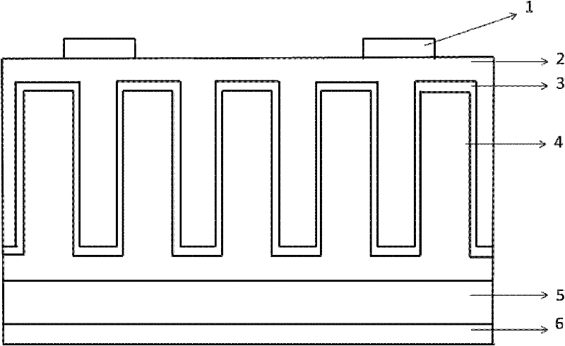
[0030] 1. Clean the p-type polysilicon wafer according to the standard semiconductor cleaning procedure (RCA method), and dry it with nitrogen gas at room temperature for later use. At normal temperature and pressure, put the prepared p-type polysilicon wafer into a solution filled with HF (20%) and AgNO 3 (0.045mol / L) etching solution in a Teflon (Teflon) beaker, sealed and reacted for 15min. Take out the sample with plastic tweezers, and rinse off the residual etching solution with plenty of deionized water. The sample was then immersed in dilute HNO 3 (20%) solution to remove reduced silver deposits. Finally, wash it dry with plenty of deionized water, and dry it with nitrogen gas for later use.
[0031] 2. Through thermal diffusion, POCl 3 As the source, the polysilicon nanowire array is n-type doped at a temperature of 930°C for 20 minutes to form a p-n junction, wherein the polysilicon nanowire structure layer 4 is n-type doped, and the polysilicon layer 5 is a p-typ...
Embodiment 2
[0039]1. Clean the p-type polysilicon wafer according to the standard semiconductor cleaning procedure (RCA method), and dry it with nitrogen gas at room temperature for later use. At normal temperature and pressure, put the prepared p-type polysilicon wafer into a solution filled with HF (20%) and AgNO 3 (0.045mol / L) etching solution in a Teflon (Teflon) beaker, sealed and reacted for 30min. Take out the sample with plastic tweezers, and rinse off the residual etching solution with plenty of deionized water. The sample was then immersed in dilute HNO 3 (20%) solution to remove reduced silver deposits. Finally, wash it dry with plenty of deionized water, and dry it with nitrogen gas for later use.
[0040] 2. Through thermal diffusion, POCl 3 As the source, the polysilicon nanowire array is n-type doped at a temperature of 930°C for 20 minutes to form a p-n junction, wherein the polysilicon nanowire structure layer 4 is n-type doped, and the polysilicon layer 5 is a p-type...
Embodiment 3
[0048] 1. Clean the p-type polysilicon wafer according to the standard semiconductor cleaning procedure (RCA method), and dry it with nitrogen gas at room temperature for later use. At normal temperature and pressure, put the prepared p-type polysilicon wafer into a solution filled with HF (20%) and AgNO 3 (0.045mol / L) etching solution in a Teflon (Teflon) beaker, sealed and reacted for 60min. Take out the sample with plastic tweezers, and rinse off the residual etching solution with plenty of deionized water. The sample was then immersed in dilute HNO 3 (20%) solution to remove reduced silver deposits. Finally, wash it dry with plenty of deionized water, and dry it with nitrogen gas for later use.
[0049] 2. Through thermal diffusion, POCl 3 As the source, the polysilicon nanowire array is n-type doped at a temperature of 930°C for 20 minutes to form a p-n junction, wherein the polysilicon nanowire structure layer 4 is n-type doped, and the polysilicon layer 5 is a p-typ...
PUM
| Property | Measurement | Unit |
|---|---|---|
| Diameter | aaaaa | aaaaa |
| Depth | aaaaa | aaaaa |
| Width | aaaaa | aaaaa |
Abstract
Description
Claims
Application Information