

Method for preparing light emitting diode
A preparation process and photolithography technology, which is applied in the direction of electrical components, circuits, semiconductor devices, etc., can solve the problems that homogeneous epitaxial substrates have not been commercialized on a large scale, the preparation of GaN thick film materials is difficult, and the price of GaN substrates is expensive. , to achieve the effect of low price, high reliability and improved crystal quality
- Summary
- Abstract
- Description
- Claims
- Application Information
AI Technical Summary
Problems solved by technology
Method used
Image


Examples
Embodiment 1
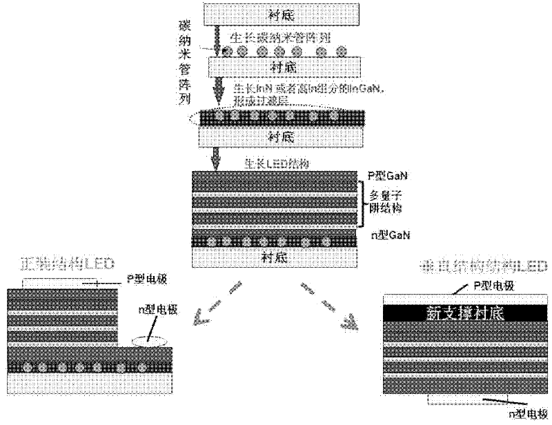
[0034] Example 1: For the preparation of the c-surface LED, refer to figure 2 :
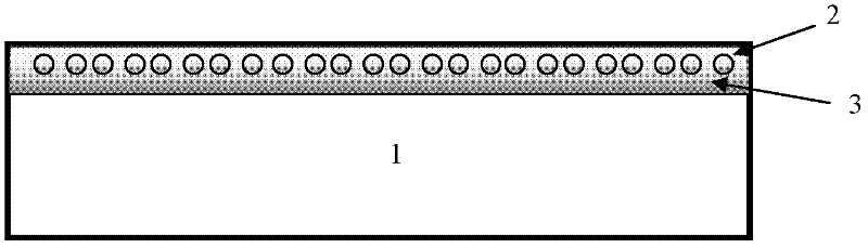
[0035] 1. The substrate can be sapphire, silicon carbide, Si and other substrates. Arrange carbon nanotubes in parallel on the substrate, the arrangement is parallel arrangement along the growth plane, the arrangement can be isoperiodic, or a periodic disordered structure, the carbon nanotubes can be a single carbon nanotube or a group of carbon nanotubes Clusters of carbon nanotubes, in various forms such as single-layer or multi-layer. The present embodiment selects the sapphire substrate of c plane, selects the single-layer carbon nanotubes arranged vertically along the reference side of the substrate at equal periods; the diameter of the carbon nanotubes is 1-100 nanometers, and this embodiment adopts 5 nanometers; the period is 1 -100 microns, preferably 1-10 microns, 2 microns are used in this embodiment.
[0036] 2. The InN material is grown by MBE growth technology to form a transition ...
Embodiment 2
[0042] Example 2: Preparation of c-plane vertical structure LED:
[0043] 1. The substrate can be sapphire, silicon carbide, Si and other substrates. Arrange carbon nanotubes in parallel on the substrate, the arrangement is parallel arrangement along the growth plane, the arrangement can be isoperiodic, or a periodic disordered structure, the carbon nanotubes can be a single carbon nanotube or a group of carbon nanotubes Clusters of carbon nanotubes, in various forms such as single-layer or multi-layer. The present embodiment selects the sapphire substrate of c plane, selects the single-layer carbon nanotubes arranged vertically along the reference side of the substrate at equal periods; the diameter of the carbon nanotubes is 1-100 nanometers, and this embodiment adopts 5 nanometers; the period is 1 -100 microns, preferably 1-10 microns, 2 microns are used in this embodiment;
[0044] An InGaN material with a high In composition is grown by MBE growth technology to form a t...
Embodiment 3
[0051] Example 3: Preparation of a c-plane LED on a thick-film GaN template:
[0052] 1. The substrate can be sapphire, silicon carbide, Si and other substrates. Arrange carbon nanotubes in parallel on the substrate, the arrangement is parallel arrangement along the growth plane, the arrangement can be isoperiodic, or a periodic disordered structure, the carbon nanotubes can be a single carbon nanotube or a group of carbon nanotubes Clusters of carbon nanotubes, in various forms such as single-layer or multi-layer. The present embodiment selects the sapphire substrate of c plane, selects the single-layer carbon nanotubes arranged vertically along the reference side of the substrate at equal periods; the diameter of the carbon nanotubes is 1-100 nanometers, and this embodiment adopts 5 nanometers; the period is 1 -100 microns, preferably 1-10 microns, 2 microns are used in this embodiment.
[0053] 2. The InN material is grown by MBE growth technology to form a transition lay...
PUM
| Property | Measurement | Unit |
|---|---|---|
| diameter | aaaaa | aaaaa |
| thickness | aaaaa | aaaaa |
| thickness | aaaaa | aaaaa |
Abstract
Description
Claims
Application Information