Variable temperature microscopic measurement system for measuring related electron-spin transportation

A technology for microscopic measurement and electron spin, which is applied in the fields of magnetic property measurement, change rate measurement, single semiconductor device testing, etc., and can solve problems such as constraints, difficulties, and expensive acquisition of liquid helium

Inactive Publication Date: 2011-11-23
INST OF SEMICONDUCTORS - CHINESE ACAD OF SCI
View PDF5 Cites 9 Cited by
  • Summary
  • Abstract
  • Description
  • Claims
  • Application Information

AI Technical Summary

Problems solved by technology

At this stage, liquid helium circulation sample chamber and liquid helium cooling superconducting coil are usually used to obtain low temperature and strong magnetic field environment. However, the expensive

Method used


Image

  • Variable temperature microscopic measurement system for measuring related electron-spin transportation
  • Variable temperature microscopic measurement system for measuring related electron-spin transportation
  • Variable temperature microscopic measurement system for measuring related electron-spin transportation

Examples


Embodiment Construction

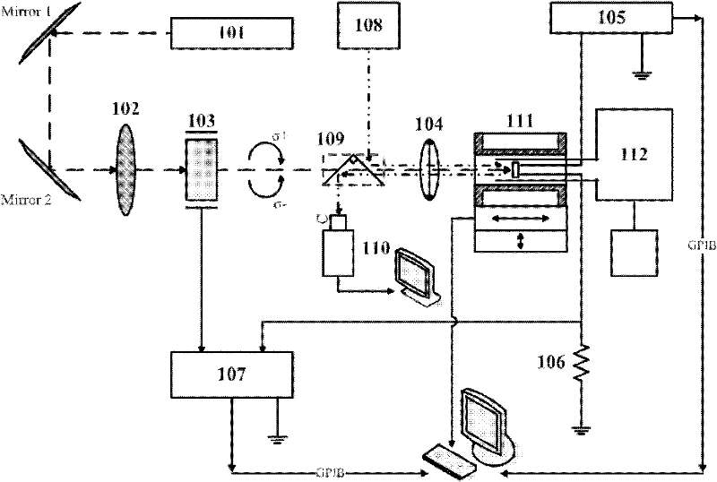
[0028] see figure 1 As shown, the present invention is a variable temperature microscopic measurement system for measuring electron spin-related transport, which system includes:

[0029] A HeNe laser 101, used to excite the sample photogenerated carriers;

[0030] A Glan-Taylor prism 102, located on the main optical path of the HeNe laser 101, converts the laser light emitted by the HeNe laser 101 into linearly polarized light;

[0031] A photoelastic modulator 103, which modulates linearly polarized light into left and right circularly polarized light modulated at a period of 50KHz;

[0032] A microscopic objective lens 104, the microscopic objective lens 104 is located on the main optical path, and is used to focus the incident laser light on the sample table;

[0033] A variable temperature liquid nitrogen Dewar sample holder 112, the variable temperature liquid nitrogen Dewar sample holder 112 is located on the main optical path, the variable temperature liquid nitrogen...


PUM


Abstract

The invention discloses a variable temperature microscopic measurement system for measuring related electron-spin transportation, which comprises an HeNe laser, a Grand taylor prism, a photoelastic modulator, a micro objective, a variable temperature liquid nitrogen Dewar sample holder, a digital voltage current source meter, a sampling resistance, a phase locked amplifier, a half-reflecting and half-transmitting lens group, a white light source, a camera, a display and a neodymium iron boron ring-shaped permanent magnet, wherein, the laser sent out by the HeNe laser is converted into linearly polarized light by the Grand taylor prism; the micro objective is used for focusing the incident lasers onto the platform surface of a sample; the variable temperature liquid nitrogen Dewar sample holder comprises a temperature control meter and a red copper cold finger which is used for fixing the sample to be detected on the top of the red copper cold finger; the control end of the digital voltage current source is connected with a computer through a general purpose interface bus (GPIB); the sampling resistance is used for extracting an alternating current voltage signal of the sample to be detected; the control end of the phase locked amplifier is connected with the computer through the GPIB; the half-reflecting and half-transmitting lens group is positioned on a main optical path; the white light source is used for observing the position on the platform surface of the sample to be detected; the camera and the display are used for displaying and outputting a platform surface image of the sample to be detected and the laser light spot position; and the neodymium iron boron ring-shaped permanent magnet is coaxially sheathed outside the red copper cold finger of the variable temperature liquid nitrogen Dewar sample holder.

Description

technical field [0001] The invention belongs to the technical field of semiconductor electrical property testing technology and magnetic material magnetic property testing technology, in particular to the spin-related transport of ferromagnetic metal-semiconductor structure (including spin injection from ferromagnetic metal to semiconductor direction and from semiconductor to iron A measurement technique for the spin-filtering) properties of magnetic metal orientations. Background technique [0002] Modern information technology uses the charge degree of freedom of electrons for information processing, and uses the spin degree of freedom of magnetic materials to store information. The emerging field of spintronics exploits these two degrees of freedom of electrons simultaneously to generate new functions, which may lead to future innovations in information technology. The spin-dependent transport process between ferromagnetic metal-semiconductor structures includes the inje...

Claims


Application Information

Patent Timeline
IPC IPC(8): G01R31/26G01R19/12G01R33/12
Inventor 李韫慧章昊肖文波吴昊谭平恒
Owner INST OF SEMICONDUCTORS - CHINESE ACAD OF SCI
Why Eureka
Try Eureka