
Method for manufacturing micro lens array based on digital mask lithography technology

A microlens array and lithography technology, applied in the field of microlens array fabrication based on digital mask lithography technology, can solve problems such as pattern distortion, reduce data volume, improve optical performance, and reduce errors. Effect

Inactive Publication Date: 2011-11-23
NANCHANG HANGKONG UNIVERSITY
View PDF0 Cites 8 Cited by
  • Summary
  • Abstract
  • Description
  • Claims
  • Application Information

AI Technical Summary

Problems solved by technology

Therefore, in the process of using digital mask lithography to make microlens arrays, it is inevitable that there will be graphic distortion.

Method used

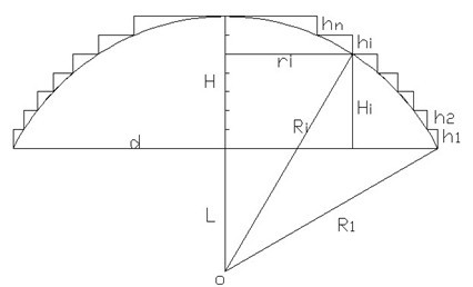
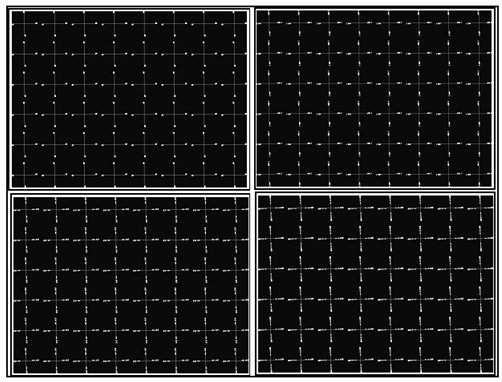

Image

  • Method for manufacturing micro lens array based on digital mask lithography technology
  • Method for manufacturing micro lens array based on digital mask lithography technology
  • Method for manufacturing micro lens array based on digital mask lithography technology

Examples


Embodiment Construction

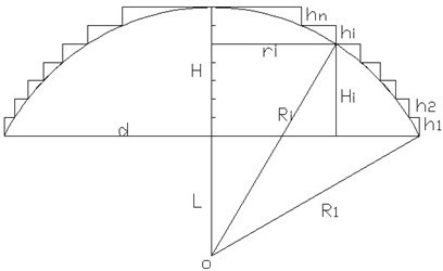
[0011] exist figure 1 In the n-order equal-height quantization of the microlens, there are:

[0012]

[0013] in Quantize the height in units;

[0014] according to figure 1 It can be seen that:

[0015]

[0016] That is, the height of the step after the actual exposure and etching, which determines the exposure amount correspondingly during the exposure process. In the present invention, equal-height quantization is adopted, so there is a multiple relationship between each exposure height, which can help us set the time interval of exposure of each mask pattern.

[0017] exist figure 1 , according to the Pythagorean theorem, we can know the relationship between the lengths of each side:

[0018]

[0019] then there is the first The radius of the plane circle corresponding to the steps:

[0020]

[0021] then there is the first The diameter of the plane circle corresponding to the steps:

[0022]

[0023] Then for the resulting diameter Carry ou...


PUM


Abstract

The invention claims a method for manufacturing a micro lens array based on a digital mask lithography technology. The method comprises the following steps of: equally dividing the height of each lens in the array into n micro elements; calculating the diameter of a plane circular corresponding to each equal stage according to the Pythagorean theorem; performing rounding off to obtain the integer and make the obtained integer be integral multiple of the single pixel of a digital micro mirror device (DMD); and obtaining an exposure image by using an imaging optimization technology, and exposing and developing to obtain an embossment structure of the micro lens array. The method has the advantages of: 1, reducing the error of the device produced by the traditional method in design, making a micro lens have more precise surface profile structure and greatly improving the optical usability of the micro lens array; 2, combining the imaging optimization technologies such as digital real-time, shaping and rotating, improving alignment precision, reducing the data quantity of masks and saving a large storage space; and 3, keeping superfine structures of more lenses so as to ensure less limitation of the shape of the surface of the lens in preparation.

Description

technical field [0001] The invention relates to a method for manufacturing a microlens array based on digital mask photolithography technology. Background technique [0002] With the development of laser technology and micro-processing technology, the development of micro-optical array device manufacturing technology is getting faster and faster. The microlens array with the characteristics of large numerical aperture, high fill factor, and high diffraction efficiency has important application value and increasingly broad development prospects in modern defense technology and other important fields. [0003] The traditional mechanical rotating mask method can produce micro-optical array devices with large numerical aperture, central axis symmetry or rotational symmetry, but the rotation speed of the mask, the precise control of time, and the precise modulation of exposure are greatly affected. The limitations, coupled with high cost and large mechanical alignment errors, ha...

Claims


Application Information

Patent Timeline
IPC IPC(8): G02B3/00G03F7/20
Inventor 高益庆钟希欢罗宁宁
Owner NANCHANG HANGKONG UNIVERSITY
Learn More