Nanopillar array-based photoelectric device and manufacturing method thereof

A nano-pillar array, optoelectronic device technology, applied in photovoltaic power generation, electrical components, semiconductor devices, etc., can solve the problems of low yield, inability to accurately control the thickness and flatness of fillers, etc., to increase yield and improve stability and device reliability, damage prevention effect

Inactive Publication Date: 2011-11-23
SUZHOU INST OF NANO TECH & NANO BIONICS CHINESE ACEDEMY OF SCI
View PDF9 Cites 20 Cited by
  • Summary
  • Abstract
  • Description
  • Claims
  • Application Information

AI Technical Summary

Problems solved by technology

However, due to the large aspect ratio of the nano-array, the capillary effect between the filler and the nano-array cannot precisely control the thickness and flatness of the filler, so that the conduction between the top layer and the active region when depositing a current spreading layer or a metal electrode The leakage channel 208 is formed or turned on, and the yield rate is low

Method used


Image

  • Nanopillar array-based photoelectric device and manufacturing method thereof
  • Nanopillar array-based photoelectric device and manufacturing method thereof
  • Nanopillar array-based photoelectric device and manufacturing method thereof

Examples


Embodiment Construction

[0034] In order to make the purpose, technical solution and advantages of the present invention clearer, the present invention will be further described in detail below in conjunction with the accompanying drawings and a preferred embodiment.

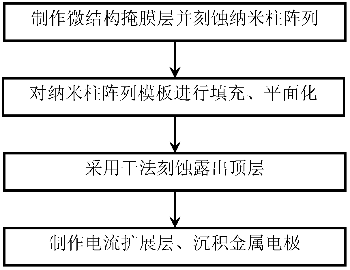
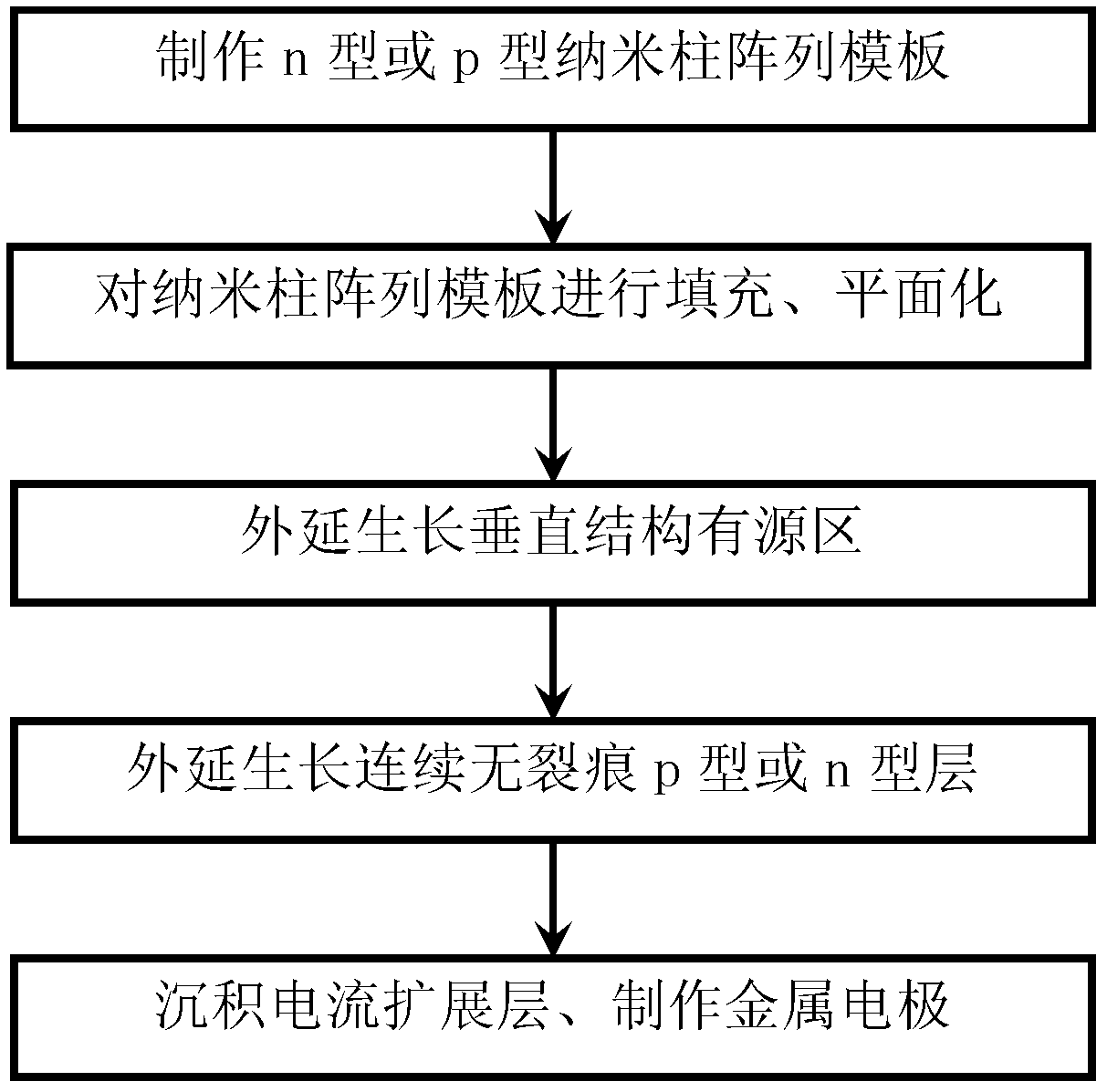
[0035] The preparation method of the photoelectric device based on the nano-column array of the present invention is illustrated by taking the nano-column array InGaN / GaN p-i-n double heterojunction solar cell structure prepared on the sapphire substrate as an example, wherein the intrinsic InGaN absorbing layer is equivalent to other photoelectric devices. source area, see Figure 3-5 , its manufacturing process includes the following main steps:

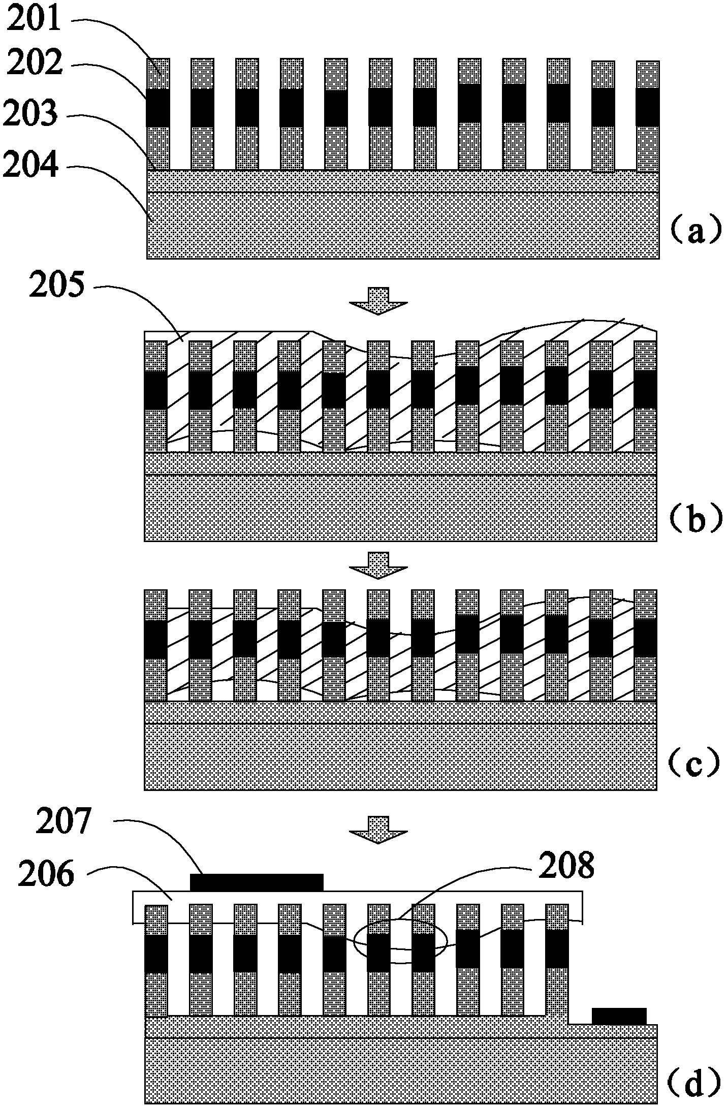
[0036] Step 1: Make a microstructure mask layer on the top layer of n-type GaN, and etch to form a nanopillar array:

[0037] Firstly, the sample is cleaned, and the substrate is placed in a plasma-enhanced chemical vapor deposition (PECVD) vacuum chamber, the temperature of the substrate i...


PUM


Abstract

The invention discloses a nanopillar array-based photoelectric device and a manufacturing method thereof. The photoelectric device comprises an n type or p type semiconductor layer of which the surface is provided with a nanopillar array structure; an active region having a vertical structure and a transverse continuous crackless p type or n type region are grown on the nanopillar array in turn; a current expansion layer is coated on the p type or n type region; and electrodes are arranged on the n type or p type semiconductor layer and the current expansion layer. The method comprises the following steps of: filling and flattening a nanopillar array template; manufacturing the active region, the p type or n type region, the current expansion layer and the electrodes and the like. The problem of leakage current in the process of manufacturing a metal electrode in the traditional nano structure photoelectric device is solved, and the problems that etching in a 'top to bottom' preparation process damages the surface of the active region and the nano structure has inconsistent orientation in a 'top to bottom' preparation method can be effectively prevented; therefore, the device has characteristics of a nano structure, and the yield, the electrical stability and reliability of the device are improved.

Description

technical field [0001] The invention relates to a photoelectric device and a preparation method thereof in the field of semiconductor material growth, in particular to a semiconductor photoelectric device based on a nano-column array template and a preparation method thereof. Background technique [0002] In order to improve the performance of optoelectronic devices and introduce new effects including quantum effects, nanostructures such as nanopillars and nanowires have been widely used in optoelectronic devices. Due to the lateral size effect, the one-dimensional nanostructure restricts the lateral movement of carriers, and the longitudinal movement becomes more efficient, enabling nanostructure-based optoelectronic devices to obtain higher carrier transport capacity, responsivity and higher At the same time, compared with the crystal film structure, the nanostructure can effectively release the lateral stress during the growth process, and obtain high-quality crystal mate...

Claims


Application Information

Patent Timeline
Patent Type & Authority Applications(China)
IPC IPC(8): H01L31/0352H01L31/04H01L31/18
CPCY02E10/50Y02P70/50
Inventor 张东炎郑新和李雪飞董建荣杨辉
Owner SUZHOU INST OF NANO TECH & NANO BIONICS CHINESE ACEDEMY OF SCI
Why Eureka
Try Eureka