MOS (Metal Oxide Semiconductor) type power device and manufacturing method thereof

A technology for power devices and manufacturing methods, which is applied in semiconductor/solid-state device manufacturing, semiconductor devices, electrical components, etc., can solve problems such as increasing the junction depth of the well region, and achieve the advantages of increasing withstand voltage, reducing bulk resistance, and reducing resistivity. Effect

Active Publication Date: 2013-06-19
BYD SEMICON CO LTD
View PDF4 Cites 0 Cited by
  • Summary
  • Abstract
  • Description
  • Claims
  • Application Information

AI Technical Summary

Problems solved by technology

Figure 4 Yes image 3 The longitudinal distribution diagram of the impurity concentration in the cross-section along the dotted line AB in the structure; it can be seen that although the impurity concentration inside the P-type well region has increased, the peak concentration on the surface of the silicon wafer still exists. , it will inevitably limit the increase of the junction depth of the well region

Method used


Image

  • MOS (Metal Oxide Semiconductor) type power device and manufacturing method thereof
  • MOS (Metal Oxide Semiconductor) type power device and manufacturing method thereof
  • MOS (Metal Oxide Semiconductor) type power device and manufacturing method thereof

Examples


Embodiment Construction

[0030] In order to make the technical problems, technical solutions and beneficial effects solved by the present invention clearer, the present invention will be further described in detail below in conjunction with the accompanying drawings and embodiments. It should be understood that the specific embodiments described here are only used to explain the present invention, not to limit the present invention.

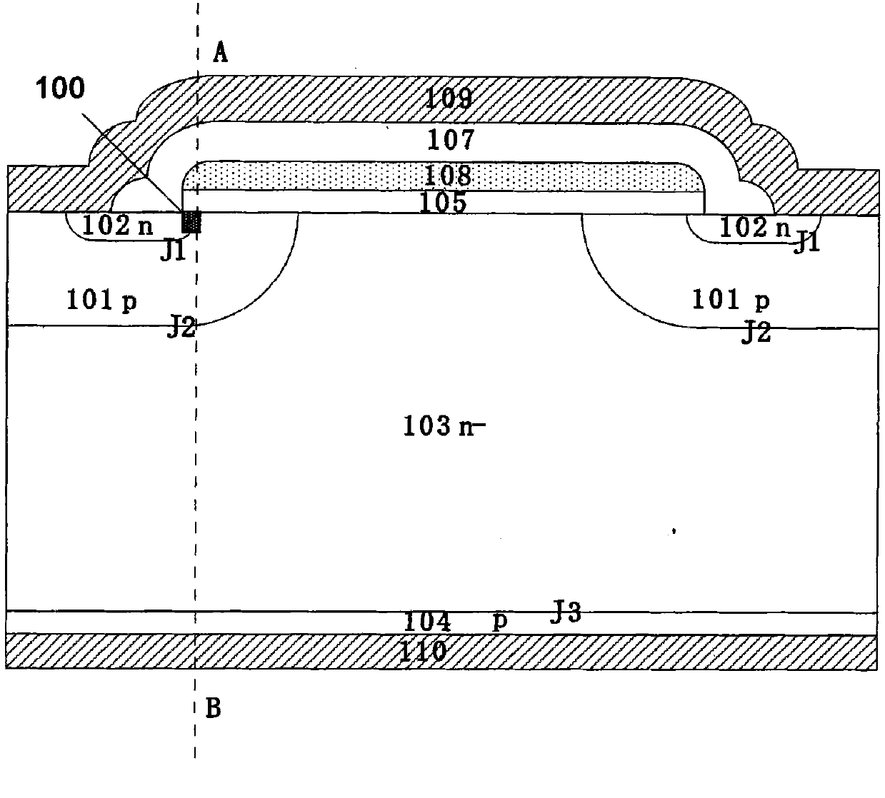
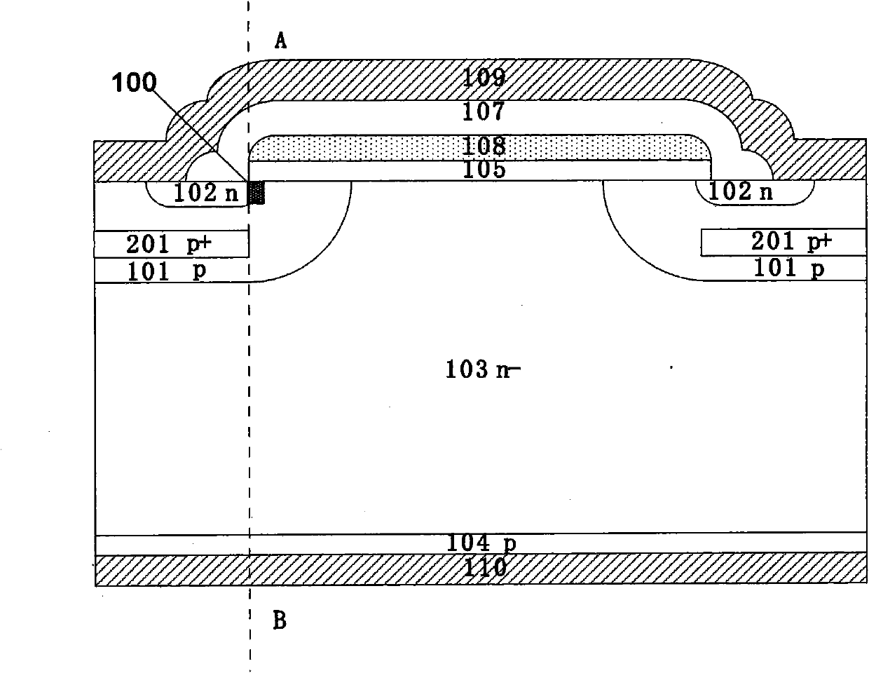
[0031] Figure 5It is a schematic structural diagram of an n-channel planar MOS power device in the first embodiment of the present invention; a MOS power device includes: a first conductivity type collector region 304; a second conductivity type drift region 303 located in the second conductivity type On the collector region of a conductivity type; the first well 301, which is selectively formed on the drift region, is opposite to the conductivity type of the drift region of the second conductivity type; the source region 302 of the second conductivity type, which is fo...


PUM


Abstract

The invention relates to an MOS (Metal Oxide Semiconductor) type power device which comprises a P-type collector region, an N-type shifting region, a P well, an N-type source region, a first insulating layer, a gate pole, a second insulating layer, an emitting electrode and a collecting electrode, wherein the N-type shifting region is located on the P-type collector region; the P well is selectively formed on the N-type shifting region and has a conduction type which is opposite to the conduction type of the N-type shifting region; the N-type source region is selectively formed on a surface area of the P well; the first insulating layer is located on the N-type shifting region and partially covers the P well; the gate pole is located on the first insulating layer; the second insulating layer covers the gate pole and partially covers the N-type source region; the emitting electrode covers the second insulating layer and is electrically connected with the P well and the N-type source region partially; the collecting electrode is located on the back side of the P-type collector region and is electrically connected with the P-type collector region; a conductive impurity concentration peak area is arranged in the P well; the impurity concentration is gradually reduced from the conductive impurity concentration peak area to the edge of the P well; and a junction bending center of the P well is arranged inside the P well. The invention also provides a manufacturing method of the MOS type power device. The inside resistivity is reduced while the demand on the length of a surface trench is met, thereby reducing the bulk resistor and reducing a latch-up effect.

Description

technical field [0001] The invention relates to a semiconductor power device, in particular to a MOS type power device and a manufacturing method thereof. Background technique [0002] Metal-oxide-semiconductor field-effect (MOS) power devices are power devices that use electric field effects to control the formation and disappearance of conductive channels, thereby realizing the on and off control of devices. Currently, they mainly include metal-oxide-semiconductor field-effect Transistors (MOSFETs) and insulated gate bipolar transistors (IGBTs) have the advantages of high operating frequency and simple control circuits, and are widely used in the field of power control. [0003] An IGBT is an element that combines the insulated gate structure of a MOS transistor with the high current density characteristics of a bipolar transistor. Unlike MOS transistors, IGBTs have a parasitic PNPN thyristor structure, where the parasitic PNPN thyristor structure includes a P+ collector ...

Claims


Application Information

Patent Timeline
Patent Type & Authority Patents(China)
IPC IPC(8): H01L29/739H01L29/36H01L21/331
Inventor 肖秀光吴海平
Owner BYD SEMICON CO LTD
Why Eureka
Try Eureka