
A Method for Cutting 170μm Silicon Wafer

A technology for silicon wafers and cutting fluids, applied in the directions of cleaning methods using liquids, chemical instruments and methods, cleaning methods and utensils, etc., can solve the problems of silicon wafer damage, cleaning, uncleanness, affecting the yield and quality of silicon wafers, etc. Achieve the effect of reducing thickness, reducing production cost, improving film yield and production efficiency

Inactive Publication Date: 2011-12-14
太仓协鑫光伏科技有限公司
View PDF6 Cites 26 Cited by
  • Summary
  • Abstract
  • Description
  • Claims
  • Application Information

AI Technical Summary

Problems solved by technology

[0007] In addition, if the degumming and cleaning process of the silicon wafer after cutting is not adopted properly, the silicon wafer will be damaged and cleaned, which will affect the yield and quality of the silicon wafer

Method used


Image

  • A Method for Cutting 170μm Silicon Wafer

Examples


Embodiment Construction

[0036] Below in conjunction with specific embodiment, further illustrate the present invention, should be understood that these embodiments are only used to illustrate the present invention and are not intended to limit the scope of the present invention, after having read the present invention, always adopt the mode of equivalent replacement or equivalent transformation to obtain The technical solutions all fall within the protection scope of the present invention.

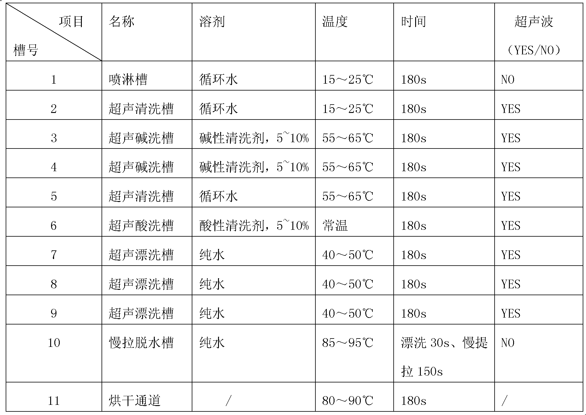
[0037] A method for cutting a 170 μm silicon wafer, comprising the steps of:

[0038] 1. Bonding silicon ingots: first put the silicon ingots and glass plates into an ultrasonic water tank for cleaning, the cleaning water temperature is 30-40°C, the cleaning time is 15min, and then in an environment of 25±3°C and humidity ≤60% , the silicon ingot and the glass plate are bonded together with glue, and the amount of glue is 0.5-0.7g / cm 2 , according to the calculation of the bonding surface of the silicon ingot an...


PUM

PropertyMeasurementUnit
Rotational viscosityaaaaaaaaaa
Densityaaaaaaaaaa
Conductivityaaaaaaaaaa

Abstract

The invention discloses a method for cutting 170 μm silicon wafers, which comprises the following steps: (1) bonding silicon ingots: using glue to bond silicon ingots and glass plates into one; (3) Set the groove distance of the guide wheel of the wire cutting machine into three sections, respectively 320±2μm, 317±2μm and 313±2μm, and use a steel wire with a diameter of 115μm to drive; step (2) The mortar prepared in step (1) carries out wire cutting to the silicon ingot and the glass plate which are bonded together in step (1); (4) degumming: use the degumming machine to separate the silicon wafer from the glass plate; (5) cleaning: remove the residue after degumming Clean metal ions and organic impurities on the surface of the silicon wafer. Compared with the prior art, the present invention has the following advantages: it realizes the cutting of 170 μm silicon wafers, reduces the thickness of the silicon wafers, improves the yield and production efficiency, and greatly reduces the production cost; the degumming and cleaning of the silicon wafers High yield and excellent quality.

Description

technical field [0001] The invention relates to a method for cutting a silicon wafer, in particular to a method for cutting a silicon wafer whose thickness specification is 170 μm. Background technique [0002] At present, in the solar energy industry, with the changes in market conditions, the price of solar silicon wafers continues to drop. In order to improve their competitiveness in the market, various companies are committed to reducing the production cost of solar silicon wafers. [0003] At present, the thickness specification standard of 156*156mm polysilicon wafer is 200±20μm. The next process of solar silicon wafer is the production of solar cells. For the solar cell industry, the most important indicator of silicon wafers is conversion efficiency (conversion efficiency = maximum output power / input power of the solar cell*100%), and the most important factors affecting the conversion efficiency are the surface quality of the silicon wafer and the minority carrier ...

Claims


Application Information

Patent Timeline
IPC IPC(8): B28D5/04B08B3/12B08B3/08
Inventor 甘大源朱海亮刘坤
Owner 太仓协鑫光伏科技有限公司
Features
  • Generate Ideas
  • Intellectual Property
  • Life Sciences
  • Materials
  • Tech Scout
  • Unparalleled Data Quality
  • Higher Quality Content
  • 60% Fewer Hallucinations
Learn More