A method of using diamond wire cut solar grade polysilicon wafers
A polycrystalline silicon wafer and diamond wire technology, which is applied in the field of solar-grade polycrystalline silicon wafers and their cutting, can solve the problems of difficulty in recycling, low cutting efficiency, waste of silicon resources, etc., so as to improve photoelectric conversion efficiency, fast cutting speed, and save silicon resources. Effect
Inactive Publication Date: 2011-12-21
江西金葵能源科技有限公司
View PDF5 Cites 24 Cited by
- Summary
- Abstract
- Description
- Claims
- Application Information
AI Technical Summary
Problems solved by technology
At present, NTC, MB, and HTC are commonly used to cut polysilicon wafers, and the free mortar cutting process is used. Due to the impurities inside the polysilicon, it is easy to cause disconnection during the cutting process, resulting in a low good rate; Silicon is difficult to recycle, causing serious environmental pollution; silicon powder is difficult to recycle, wasting precious silicon resources; the cutting efficiency is relatively low, and there are also a large number of loss layers on the surface of the silicon wafer, which affects the performance of the cell
Method used
View moreImage
Smart ImageViewing Examples

Examples
Embodiment Construction
Login to View More PUM
 Abstract
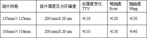
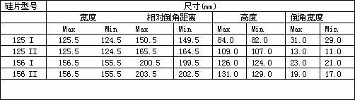
The invention discloses a method for cutting solar-grade polysilicon wafers using diamond wire cutting. The polysilicon rods are glued to the sticks after being squared, ground and ground. The resin strip is fixed on the bonding board, and then the bonding board and the polysilicon rod are put into the working cabin, the cutting fluid is preheated and circulated in the working cabin, and the diamond wire is cut into polysilicon wafers, and the polysilicon wafers are placed upside down on the degumming equipment It is made by degumming, ultrasonic cleaning, and drying. The present invention does not produce indole-like cut marks on the surface of the polycrystalline silicon sheet, improves the photoelectric conversion efficiency of the polycrystalline silicon sheet, has high diamond wire cutting speed, high dimensional accuracy of the cut polycrystalline silicon sheet, small error, and a qualified rate of more than 95%. The silicon powder produced by cutting can be recycled, saving precious silicon resources.
Description
technical field [0001] The invention relates to a solar-grade polycrystalline silicon chip cut by diamond wire and a cutting method thereof. Background technique [0002] Solar polycrystalline silicon wafers are used in solar cells, and polycrystalline silicon rods are processed into silicon wafers by wire cutting machines. The difference between monocrystalline silicon and polycrystalline silicon mainly lies in the internal grain orientation. If grains with the same crystal plane orientation grow, it is monocrystalline silicon; otherwise, it is polycrystalline silicon. At present, NTC, MB, and HTC are commonly used to cut polysilicon wafers, and the free mortar cutting process is used. Due to the impurities inside the polysilicon, it is easy to cause disconnection during the cutting process, resulting in a low good rate; Silicon is difficult to recycle, causing serious environmental pollution; silicon powder is difficult to recycle, wasting precious silicon resources; the ...
Claims
Login to View More Application Information
Patent Timeline
 Patent Type & Authority Applications(China)
IPC IPC(8): B28D5/04
Inventor 于景俞建业曾斌叶平欧阳思周汤玮胡凯
Owner 江西金葵能源科技有限公司
Features
- R&D
- Intellectual Property
- Life Sciences
- Materials
- Tech Scout
- Unparalleled Data Quality
- Higher Quality Content
- 60% Fewer Hallucinations
Learn More Browse by: Latest US Patents, China's latest patents, Technical Efficacy Thesaurus, Application Domain, Technology Topic, Popular Technical Reports.
© 2025 PatSnap. All rights reserved.Legal|Privacy policy|Modern Slavery Act Transparency Statement|Sitemap|About US| Contact US: help@patsnap.com