Transmissive metal grating coupling spr detection chip and detector

A metal grating and detection chip technology, applied in the direction of transmittance measurement, etc., can solve the problem of increasing the volume of the detector, and achieve the effects of reducing the volume and cost of the instrument, high sensitivity, and convenient portability and operation

Inactive Publication Date: 2011-12-21
SUZHOU INST OF NANO TECH & NANO BIONICS CHINESE ACEDEMY OF SCI
View PDF3 Cites 20 Cited by
  • Summary
  • Abstract
  • Description
  • Claims
  • Application Information

AI Technical Summary

Problems solved by technology

This coupling method is only smaller than the size of the chip in the prism coupling method, but it still needs to adjust the angle of the incident light and increase the size of the detector

Method used


Image

  • Transmissive metal grating coupling spr detection chip and detector
  • Transmissive metal grating coupling spr detection chip and detector
  • Transmissive metal grating coupling spr detection chip and detector

Examples


Embodiment 1

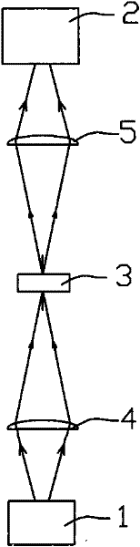
[0030] Embodiment 1 refers to figure 1 The transmission type metal grating coupling SPR detector includes a light source 1, a spectrometer 2 and a chipset composed of more than one transmission type metal grating coupling SPR detection chip 3, which is placed on the optical path formed between the light source 1 and the spectrometer 2 , and between the chipset, the light source 1 and the spectrometer 2, focusing prisms 4 and 5 are respectively provided.

[0031] The aforementioned light source is preferably a near-infrared laser, and the wavelength range of the emitted light is determined according to the grating structure in the detection chip 3 .

[0032] The aforementioned spectrometer is preferably a spectrometer with optical fiber transmission, and the wavelength range of the received light corresponds to the wavelength of the emitted light of the laser, for example, it can be in the range of 350-1200nm.

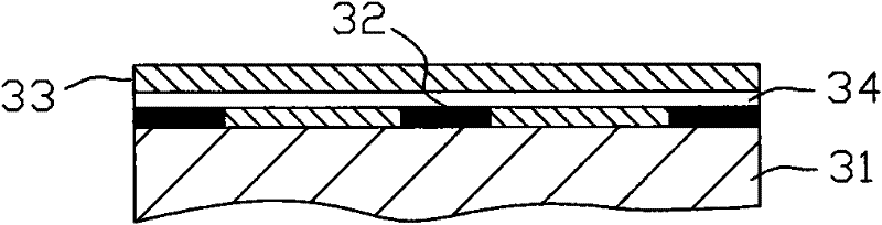
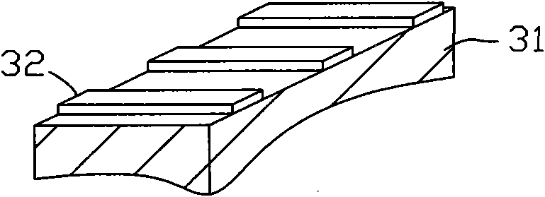
[0033] The aforementioned detection chip 3 includes a light-trans...

Embodiment 2

[0046] Embodiment 2 The structure, preparation and application methods of the transmission type metal grating coupling SPR detection chip in this embodiment are basically the same as those in the embodiment, but no modification is made on the surface of the metal grating coupling layer. When it is applied, after the test platform is built, the test sample can be directly dropped into the microfluidic channel in the chip, and then the change of the concentration of a certain sample can be tested.

[0047] For example, detecting the shift of the resonance peak caused by the change of the dielectric constant of the medium layer caused by the volatilization of alcohol. First, a certain concentration of ethanol is dropped on the surface of the metal coupling layer with a grating structure, and a resonance peak is obtained according to its transmission spectrum. As the ethanol concentration on the surface of the gold film gradually decreases with time, the dielectric constant of the...


PUM

PropertyMeasurementUnit
thicknessaaaaaaaaaa

Abstract

The invention discloses a transmission-type metal grating coupling SPR detection chip and a detection instrument, which are used for detecting target analytes in microfluids. The detection chip includes: a light-transmitting substrate; a metal film layer with a grating structure formed on the substrate; and a microfluidic layer covering the surface of the metal film layer, and microfluidic channels are distributed in the microfluidic layer, and The microfluidic channels are in contact with the metal membrane surface. The detector includes a light source, a spectrometer and the aforementioned detection chip. The invention utilizes the local characteristics of the surface plasmons and the frequency selection characteristics of the grating to realize signal enhancement and filtering, and detects the change of the peak value of the transmittance by measuring the change of the peak value of the transmittance after the incident light is coupled through the grating. Changes in biological information or concentration. The invention does not need to change the angle of the incident angle during detection, and has the advantages of real-time monitoring, high sensitivity, stability and speed, small size of the instrument, and convenient portability and operation.

Description

technical field [0001] The invention particularly relates to a transmission type metal grating coupled SPR detection chip and a detection instrument in the technical field of surface plasmon resonance (SPR) biological and chemical detection. Background technique [0002] In 1983, Nylander and Liedberg used SPR technology in gas detection and biosensors. Since then, this technology has attracted the attention of researchers and has continued to develop rapidly. Various types of new types of detection of physical, chemical, and biomass have emerged. SPR sensing structures and devices. SPR technology has the characteristics of high sensitivity, label-free, stable, fast, convenient and real-time, and is especially suitable for the study of biomolecular interactions. [0003] SPR technology is based on the physical phenomenon of light waves interacting with metal electrons. When the incident light interacts with the free electrons on the metal surface, the incident light wave w...

Claims


Application Information

Patent Timeline
Patent Type & Authority Applications(China)
IPC IPC(8): G01N21/59
Inventor 张宝顺刘帆李海军付凯刘冬杨乐臣
Owner SUZHOU INST OF NANO TECH & NANO BIONICS CHINESE ACEDEMY OF SCI
Why Eureka
Try Eureka