Dynamic Body Bias Type C Inverter and Its Application

A type of inverter and body bias technology, which is applied in the direction of pulse generation, electrical components, components of electric pulse circuit, etc., can solve the problems of large size and high static power consumption

Active Publication Date: 2011-12-21
ZHEJIANG UNIV
View PDF6 Cites 19 Cited by
  • Summary
  • Abstract
  • Description
  • Claims
  • Application Information

AI Technical Summary

Problems solved by technology

However, the problem with the above-mentioned gain bootstrap type C inverter is that in order to ensure that the gain bootstrap type C inverter has sufficient bandwidth and slew rate in the high slew rate state (especially in SS process corner, low power supply voltage and low temperature), the size of the gain bootstrap C-type inverter input tube is generally relatively large, and the PMOS body potential modulation module and the NMOS body potential modulation module respectively apply positive voltage to the PMOS input tube M1 and NMOS input tube M2. Body-biased, and these measures lead to unnecessary and high static power consumption when the gain-bootstrapped Class-C inverter is in the subthreshold state

Method used


Image

  • Dynamic Body Bias Type C Inverter and Its Application
  • Dynamic Body Bias Type C Inverter and Its Application
  • Dynamic Body Bias Type C Inverter and Its Application

Examples


Embodiment 1

[0025] Embodiment 1 Dynamic Body Bias Type C Inverter

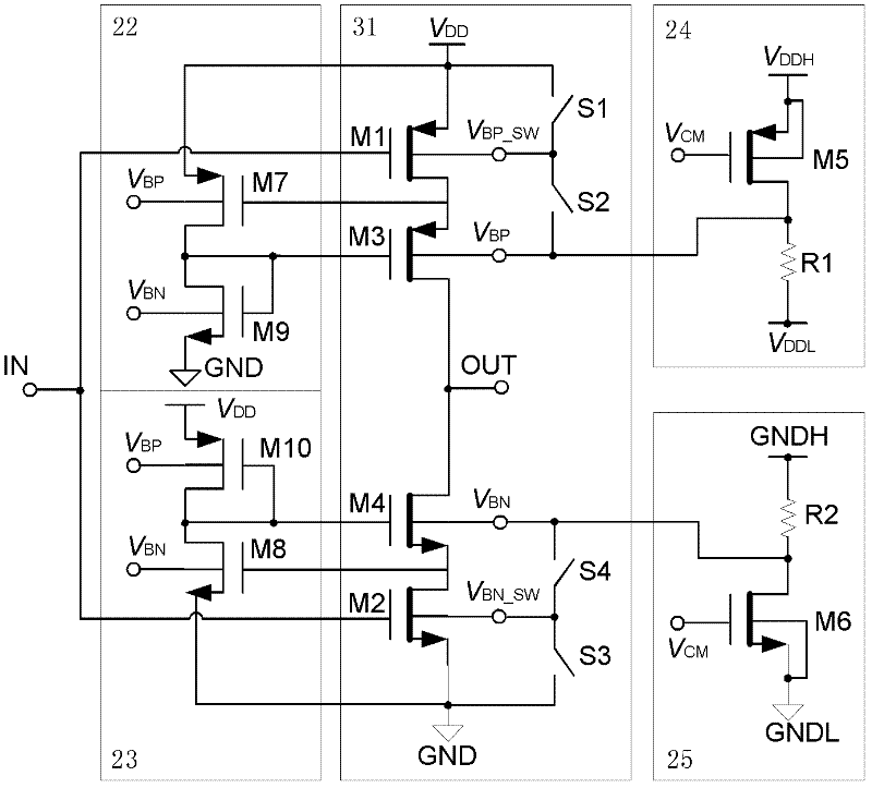
[0026] A dynamic body-bias type C-type inverter, its circuit structure diagram is attached image 3 As shown, it includes a switch body bias type C-type inverter 31 , a first gain bootstrap module 22 , a second gain bootstrap module 23 , a PMOS body potential modulation module 24 and an NMOS body potential modulation module 25 .

[0027] The switching body bias type C-type inverter 31 adopts a cascode structure, and it is composed of a first PMOS transistor M1, a second PMOS transistor M3, a first NMOS transistor M2, a second NMOS transistor M4 and four switches. To realize the operation amplification function.

[0028] Wherein, the first PMOS transistor M1 and the first NMOS transistor M2 are respectively the PMOS and the NMOS input transistors of the above-mentioned dynamic body-bias type C-type inverter, and the gate terminal of the first PMOS transistor M1 is connected to the gate terminal of the first NMOS transisto...

Embodiment 2

[0039] Embodiment 2 Pseudo-differential structure switched capacitor integrator using dynamic body bias type C-type inverter

[0040] A pseudo-differential structure switched capacitor integrator, as attached Figure 4 As shown, it includes two dynamic body-bias type C-type inverters 41 and two common-mode feedback circuits 42 in Embodiment 1, wherein the two dynamic body-bias type C-type inverters 41 are respectively located in the switched capacitor The positive and negative branches of the integrator are differentially symmetrical to form a pseudo-differential structure, and the two common-mode feedback circuits 42 respectively form common-mode feedback in the positive and negative branches of the switched capacitor integrator. The switched capacitor integrator is divided into a sampling phase and an integral phase in actual work, and is controlled by two non-overlapping clocks of p1 and p2.

[0041] During the sampling phase, the input signal IN is sampled to the capacito...

Embodiment 3

[0045] Embodiment 3 A 2-1 cascaded Sigma-Delta analog-to-digital converter using a switched capacitor integrator with a pseudo-differential structure

[0046] A 2-1 cascaded Sigma-Delta analog-to-digital converter, including a 2-1 cascaded analog modulator and a digital decimation filter, wherein the circuit structure diagram of the 2-1 cascaded analog modulator is as attached Figure 6 As shown, it includes a first-level modulator and a second-level modulator, and the second-level modulator is cascaded with the first-level modulator to modulate the quantization error generated by the previous level; the first-level modulator is a second-order It consists of two switched capacitor integrators based on the pseudo-differential structure in Embodiment 2 (i.e. the first integrator 62 and the second integrator 63), the first comparator 67 and the first feedback DAC 65, the first integrator 62 and the second integrator 63 are connected in series to form a second-order single-loop st...


PUM


Abstract

The invention discloses a dynamic body biasing class-C inverter and application thereof. The dynamic body biasing class-C inverter provided by the invention comprises a switch body biasing class-C inverter, a first gain boosting module, a second gain boosting module, a P-channel metal oxide semiconductor (PMOS) body potential modulation module and an N-channel metal oxide semiconductor (NMOS) body potential modulation module, wherein the body ends of two input tubes of the switch body biasing class-C inverter are independently led out to be connected with a switch and perform dynamic body biasing by the switching of the switch, so that the two input tubes have different parameters such as threshold value voltages, transconductances and the like at different switch phases. The inverter hasthe advantages of high DC gain, relatively higher process fluctuation resistance, relatively higher power voltage disturbance resistance, relatively higher temperature deviation resistance and the like, simultaneously greatly reduces the static power consumption of the class-C inverter in a sub-threshold value state, can form a switching capacitance integrator having a pseudo-differential structure, and is applied to application occasions such as 2-1 cascaded Sigma-Delta analogue-to-digital converters and the like with extremely low power consumption and high accuracy.

Description

technical field [0001] The invention belongs to the technical field of integrated circuits, and in particular relates to a class-C inverter and an application circuit thereof. Background technique [0002] In traditional analog circuit design, the operational amplifier is the main functional module, and it is widely used in sample-and-hold, algebraic operations, common-mode feedback, and buffer circuits. At the same time, the operational amplifier is also the main power consumption module in the analog circuit. At present, low voltage and low power consumption are the mainstream trend in the development of analog circuit design. Therefore, how to implement an operational amplifier that meets the specification requirements in a low-voltage and low-power consumption environment has become the focus and difficulty of analog circuit design. [0003] It is a new low-voltage low-power circuit design technique to replace the traditional operational amplifier with a class-C invert...

Claims


Application Information

Patent Timeline
Patent Type & Authority Applications(China)
IPC IPC(8): H03K3/01H03K3/356
Inventor 罗豪韩雁张泽松梁国廖璐虞春英
Owner ZHEJIANG UNIV
Why Eureka
Try Eureka