A Ferroelectric Thin Film Gate Enhanced Gan Heterojunction Field Effect Transistor

A heterojunction field effect, ferroelectric thin film technology, applied in the field of microelectronics, can solve the problems of difficult to accurately control the thickness of the AlGaN barrier layer, difficult to monitor the etching rate, etc., to achieve simple structure, enhanced modulation effect, and stability. and high reliability

Inactive Publication Date: 2011-12-28
UNIV OF ELECTRONICS SCI & TECH OF CHINA
View PDF5 Cites 12 Cited by
  • Summary
  • Abstract
  • Description
  • Claims
  • Application Information

AI Technical Summary

Problems solved by technology

[0007] Although this method is effective, its biggest problem is that the thickness of the AlGaN barrier layer under the gate region is difficult to accurately control due to the difficulty in monitoring the etch rate.
However, according to the reports in the existing literature, the existing ferroelectric thin film / GaN heterojunction semiconductor devices (ferroelectric thin film as the gate dielectric material) all show the characteristics of normally on, that is, they belong to depletion mode devices.
In particular, the special preparation process conditions (such as high temperature and oxygen atmosphere conditions) of most ferroelectric oxide films will greatly increase the instability of devices prepared by the above technology

Method used


Image

  • A Ferroelectric Thin Film Gate Enhanced Gan Heterojunction Field Effect Transistor
  • A Ferroelectric Thin Film Gate Enhanced Gan Heterojunction Field Effect Transistor
  • A Ferroelectric Thin Film Gate Enhanced Gan Heterojunction Field Effect Transistor

Examples


Embodiment Construction

[0024] The present invention will be further described below in conjunction with the accompanying drawings and specific embodiments.

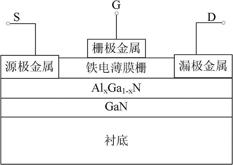
[0025] A ferroelectric thin film gate enhanced GaN heterojunction field effect transistor, such as figure 1 As shown, including the GaN film on the substrate surface with (0001) crystal orientation; the Al on the GaN film surface with (0001) crystal orientation x Ga 1-x N film, where 0x Ga 1-x N film and GaN film form a GaN heterojunction; in the Al x Ga 1-xThere are gate, source, and drain electrodes on the N film, wherein the gate electrode is located between the source electrode and the drain electrode, and between the gate electrode and the Al x Ga 1-x There is a gate dielectric film between the N films; it is characterized in that the gate dielectric film is either LiNbO 3 (LNO) ferroelectric thin film, or LiTaO 3 (LTO) ferroelectric thin film, or LNO or LTO ferroelectric thin film doped with M element. Wherein, the doping element ...


PUM


Abstract

The invention discloses a ferroelectric film grid reinforced GaN heterojunction field effect transistor and belongs to the technical field of microelectronics. The ferroelectric film grid reinforced GaN heterojunction field effect transistor comprises a GaN heterojunction formed by a (0001) crystal orientation GaN film and an AlxGal-xN (x is more than 0 but less than and equal to 1.) film, wherein a grid electrode, a source electrode and a drain electrode are formed on the AlxGal-xN film; a grid medium film is arranged between the grid electrode and the AlxGal-xN film; and the grid medium film may be a LiNbO3(LNO) ferroelectric film, a LiTaO3(LTO) ferroelectric film, or an M element-doped LNO or LTO ferroelectric film. Due to the ferroelectric spontaneous polarization in the LNO or LTO ferroelectric film in the C+ direction, 2DEG in an AlGaN/GaN heterojunction is completely exhausted, so that the ferroelectric film grid reinforced GaN heterojunction field effect transistor has a characteristic of normal close, namely a reinforced apparatus is formed; and the ferroelectric film grid reinforced GaN heterojunction field effect transistor has the characteristics of simple structure, simple implementing process, high repeatability and high stability and reliability.

Description

technical field [0001] The invention belongs to the technical field of microelectronics, relates to a ferroelectric functional film material and a semiconductor device, in particular to an enhanced GaN heterojunction field effect transistor. Background technique [0002] As a new type of wide-bandgap semiconductor material, GaN has the characteristics of large bandgap, high breakdown electric field, high thermal conductivity, high carrier mobility, and strong radiation resistance. It is widely used in microelectronics and optoelectronic devices. Wide range of applications. Based on its own strong piezoelectric polarization and spontaneous polarization, in the case of non-intentional doping, AlGaN / GaN heterojunction can form a concentration of up to 10 13 cm -2 two-dimensional electron gas. Therefore, GaN-based materials have extremely broad application prospects in the fields of high-power density, high-frequency, and high-speed electronic devices. [0003] However, sinc...

Claims


Application Information

Patent Timeline
Patent Type & Authority Applications(China)
IPC IPC(8): H01L29/778H01L29/51
Inventor 朱俊郝兰众李言荣张万里
Owner UNIV OF ELECTRONICS SCI & TECH OF CHINA
Why Eureka
Try Eureka