Thin film transistor and display device

A technology of thin film transistors and interlayer insulating films, applied in the field of display devices, can solve problems such as short circuit, interlayer insulating film coverage, source and drain open circuits, etc., to achieve improved reliability, high-quality display, and suppression of failures Effect

Inactive Publication Date: 2012-01-11
JOLED INC
View PDF11 Cites 35 Cited by
  • Summary
  • Abstract
  • Description
  • Claims
  • Application Information

AI Technical Summary

Problems solved by technology

[0008] However, in Document 1 and Document 2, after etching the gate electrode and the gate insulating film, the interlayer insulating film is formed, so there are cases where the gate electrode and the gate insulating film corresponding to the etching are formed large step of the total thickness, and the step is difficult to be covered by an interlayer insulating film made only of an insulating film by the usual plasma CVD method
Therefore, there is a disadvantage that failures such as open or short circuits of the source and drain formed later are prone to occur.
In addition, in the above-mentioned document 3, after etching the channel protective film, an interlayer insulating film is formed, therefore, a step corresponding to the thickness of the channel protective film after etching is formed, so there is a difference from that of the documents 1 and 2. Disadvantages Similar Disadvantages

Method used


Image

  • Thin film transistor and display device
  • Thin film transistor and display device
  • Thin film transistor and display device

Examples


no. 1 approach

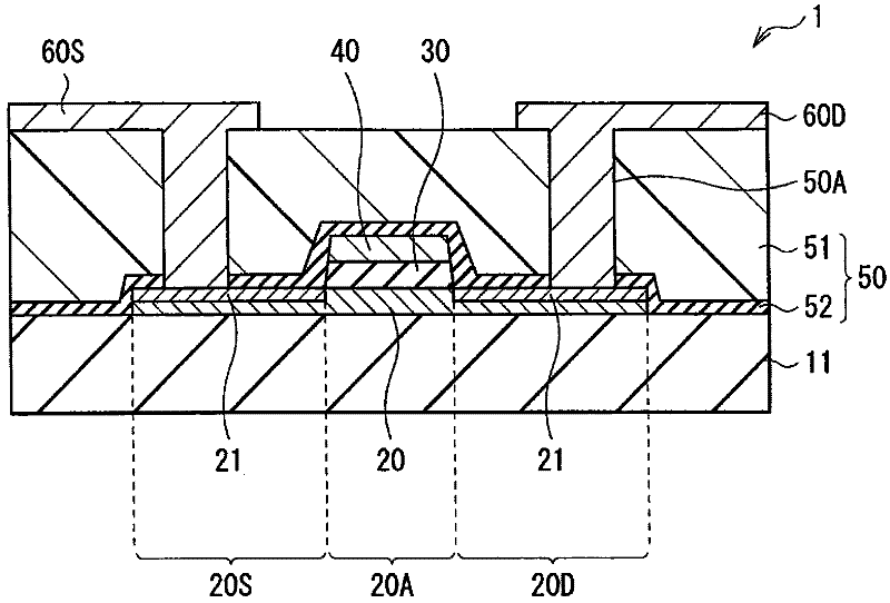
[0070] figure 1 The cross-sectional structure of the thin film transistor 1 according to the first embodiment of the present invention is illustrated. The thin film transistor 1 is used as a driving element of a liquid crystal display, an organic EL display, etc., and the thin film transistor 1 has, for example, a top-gate (staggered) structure in which an oxide semiconductor film 20 , a gate The insulating film 30, the gate electrode 40, the interlayer insulating film 50, the source electrode 60S, and the drain electrode 60D.

[0071] The substrate 11 is made of, for example, a glass substrate, a plastic film, or the like. Examples of plastic materials include PET (polyethylene terephthalate), PEN (polyethylene naphthalate), and the like. In the sputtering method described later, the oxide semiconductor film 20 is formed without heating the substrate 11, and therefore, an inexpensive plastic film can be used. In addition, the substrate 11 may be a metal substrate made of s...

example 1

[0118] Figure 6A ~ Figure 6C as well as Figure 7 The manufacturing method of the thin film transistor 1 according to Modification 1 of the present invention is illustrated in process order. This method differs from the method of the first embodiment in that the first inorganic insulating film 52 is formed by laminating the metal film 52A and the metal oxide film 52B and oxidizing the metal film 52A. It should be noted that referring to Figure 2A ~ Figure 2C The portion overlapping with the manufacturing process of the first embodiment will be described.

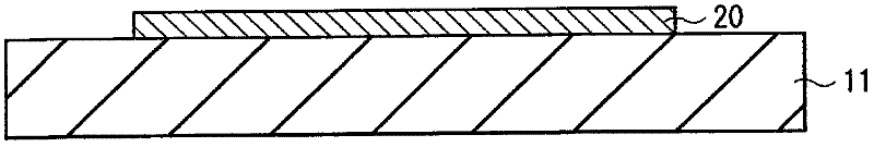
[0119] First, in a method similar to the first embodiment, by Figure 2A ~ Figure 2C In the shown process, the oxide semiconductor film 20 , the gate insulating film 30 and the gate electrode 40 are formed on the substrate 11 .

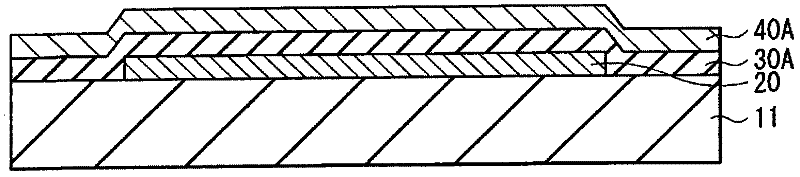
[0120] Next, if Figure 6A As shown, on the surfaces of the oxide semiconductor film 20, the gate insulating film 30, and the gate electrode 40, for example, by a sputtering method, a materia...

example 4

[0150] Figure 10 A cross-sectional configuration of a thin film transistor 1A according to Modification 4 of the present invention is illustrated. This thin film transistor 1A has a configuration similar to that of the thin film transistor 1 of the first embodiment except that the oxide semiconductor film 20 has a laminated structure including an amorphous film 22 and a crystallized film 23, and has a structure similar to that of the first embodiment. operation and effect. Accordingly, corresponding elements are given the same reference numerals as those of the first embodiment and explained.

[0151] The substrate 11 , the gate insulating film 30 , the gate electrode 40 , the interlayer insulating film 50 , the source 60S, and the drain 60D are similar to those in the first embodiment.

[0152] The oxide semiconductor film 20 has a stacked structure including an amorphous film 22 and a crystallized film 23 . The source 60S and the drain 60D are provided in contact with th...


PUM


Abstract

A thin film transistor allowed to suppress a failure caused by an interlayer insulating film and improve reliability of a self-alignment structure, and a display device including this thin film transistor are provided. The thin film transistor includes: a gate electrode; an oxide semiconductor film having a channel region facing the gate electrode, and having a source region on one side of the channel region, and a drain region on the other side of the channel region; an interlayer insulating film provided in contact with the oxide semiconductor film as well as having a connection hole, and including an organic resin film; and a source electrode and a drain electrode connected to the source region and the drain region, respectively, via the connection hole.

Description

[0001] Cross References to Related Applications [0002] This application contains subject matter related to and claims priority from Japanese Patent Application JP2010-152754 filed in the Japan Patent Office on Jul. 5, 2010, the entire content of which is hereby incorporated by reference. technical field [0003] The present invention relates to a thin film transistor (TFT) using an oxide semiconductor and a display device including the TFT. Background technique [0004] In a liquid crystal display or an organic EL (Electro Luminescence) display employing an active drive system, thin film transistors are used as drive elements, and charges corresponding to signal voltages for writing images are held in holding capacitors. However, when a parasitic capacitance existing in an intersection region between a gate and a source or a drain of a thin film transistor becomes large, signal voltage fluctuates, which may result in deterioration of image quality. [0005] Specifically, ...

Claims


Application Information

Patent Timeline
Patent Type & Authority Applications(China)
IPC IPC(8): H01L29/786H01L29/423H01L29/06H05B44/00
CPCH01L29/78618H01L29/7869H01L29/78606H01L29/78636
Inventor 诸沢成浩
Owner JOLED INC
Why Eureka
Try Eureka