Copper indium gallium selenide (CIGS) solar cell and making method thereof

A technology of solar cells and manufacturing methods, applied in the direction of final product manufacturing, sustainable manufacturing/processing, circuits, etc., can solve problems such as settlement, unfavorable solar cell photoelectric conversion efficiency, focal length or point maximum, etc., to increase light absorption volume effect

Inactive Publication Date: 2012-01-11
GCSOL TECH
View PDF4 Cites 5 Cited by
  • Summary
  • Abstract
  • Description
  • Claims
  • Application Information

AI Technical Summary

Problems solved by technology

[0003] The previous technology related to CIGS solar cells, such as the Light absorbing layer producing method patent disclosed in US Patent No. 7018858, uses a double-target sputtering method deposition equipment for depositing a precursor layer, and adopts a double-target vertical face-to-face setting The coating method of co-sputtering (co-sputter) is used, but because the substrate is placed under the target in this method, if there are pollution particles generated during the deposition process, the disadvantages of the pollution particles are prone to settle down to the substrate
[0004] Another example is the photovoltaic receiver patent disclosed in Taiwan Patent No. 200917508. The d

Method used


Image

  • Copper indium gallium selenide (CIGS) solar cell and making method thereof
  • Copper indium gallium selenide (CIGS) solar cell and making method thereof
  • Copper indium gallium selenide (CIGS) solar cell and making method thereof

Examples


Embodiment Construction

[0040] In order to illustrate the structure of the CIGS solar cell of the present invention more clearly, a preferred embodiment is given and described in detail with accompanying drawings as follows.

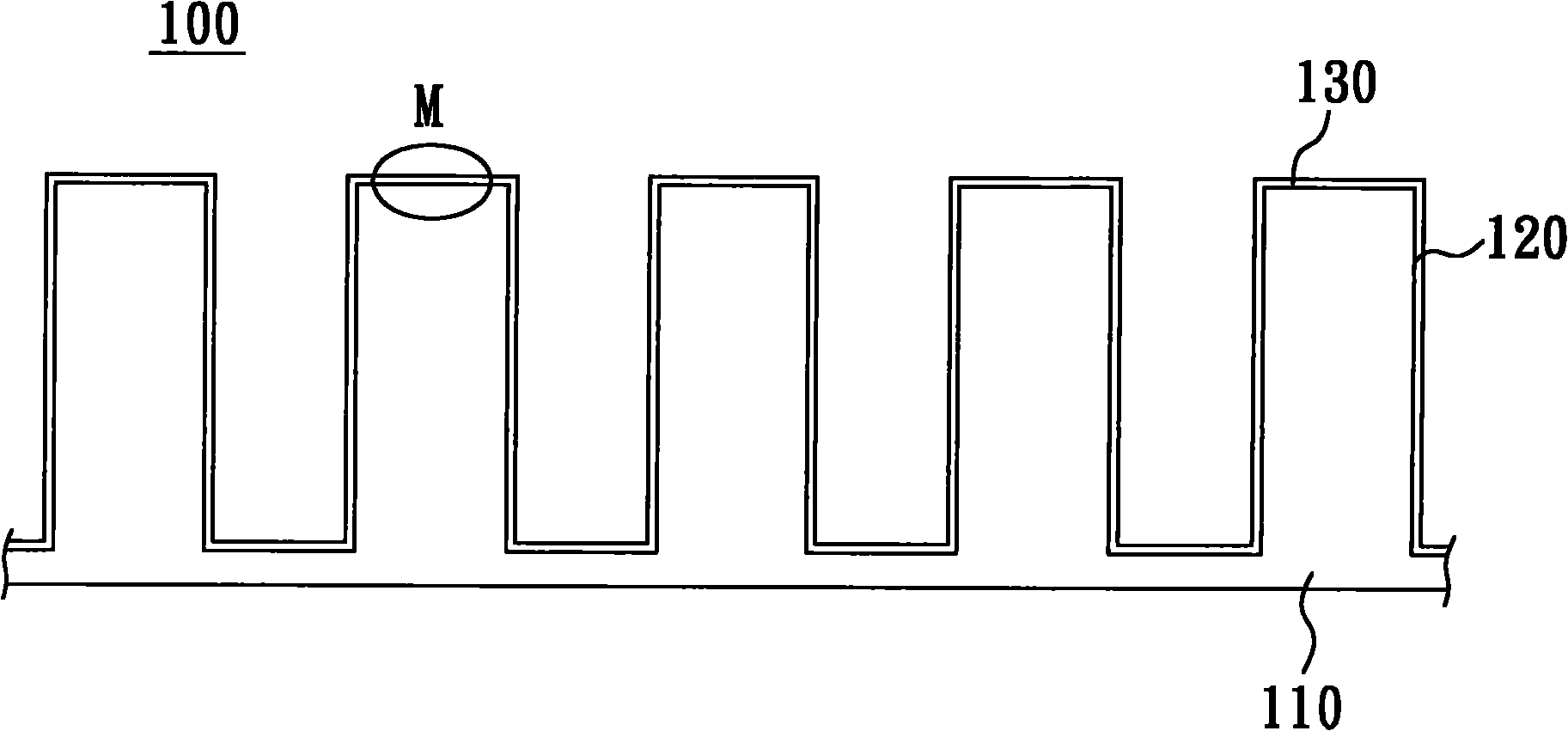
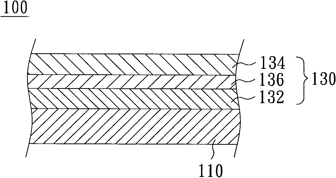
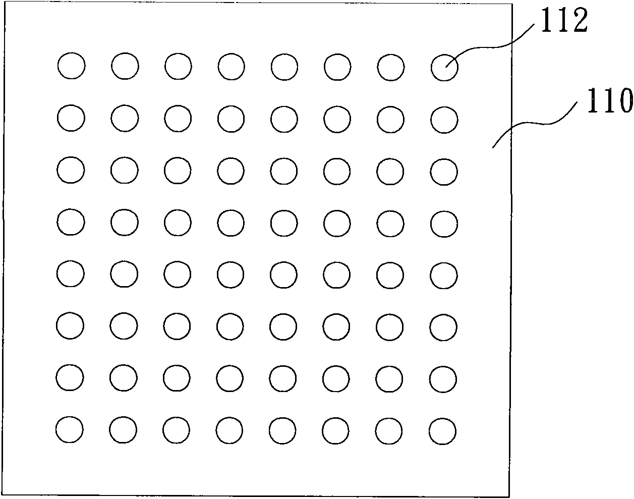
[0041] Please refer to Figure 1A , 1B , 2A and 2B are a preferred embodiment of the present invention, which respectively depict a schematic cross-sectional view of a CIGS solar cell of the present invention, a partial cross-sectional view, a top view of a glass substrate of the present invention, and Figure 2A Side view of the glass substrate. in:

[0042] The CIGS solar cell 100 includes a glass substrate 110 , a light absorbing surface 120 and a photoelectric conversion structure 130 . At least one surface of the glass substrate 110 includes a plurality of arrayed concave-convex portions 112, and the distance from the topmost to the bottommost end of each arrayed concave-convex portion 112 is a predetermined depth h. In this embodiment, the predetermined depth h is More...


PUM


Abstract

The invention discloses a copper indium gallium selenide (CIGS) solar cell and a making method thereof. The CIGS solar cell comprises a glass substrate, a light absorption surface and a photoelectric conversion structure; at least one surface of the glass substrate is provided with a plurality of array concave-convex parts; the light absorption surface comprises a set of the surfaces of topmost ends of the array concave-convex parts, the surfaces extending to bottommost ends from the topmost ends of the array concave-convex parts and the surface of a bottommost-end substrate of the array concave-convex parts except the array concave-convex parts; and the photoelectric conversion structure consists of an n-type semiconductor layer and a p-type semiconductor layer of a CIGS compound, and an i-type semiconductor layer positioned between the n-type semiconductor layer and the p-type semiconductor layer. In the invention, light absorption quantity is increased by increasing a light absorption area, and the photoelectric conversion efficiency of the CIGS solar cell is improved by combing the design of an n-i-p structure, so the production cost is reduced, and the economic value of the solar cell is improved.

Description

technical field [0001] The present invention relates to a battery and its manufacturing method, and in particular to a solar cell and its manufacturing method. Background technique [0002] Solar energy is an environmentally friendly renewable energy that can be converted into other forms of energy such as heat and electricity, and solar cells are used in a wide range of applications, ranging from large power generation systems to small consumer electronics, but solar energy is economically Competitive renewable energy is still hindered by the low efficiency of solar cells when converting light energy into electrical energy. Therefore, it has become an important aspect of solar cells to effectively improve the power generation efficiency of solar cells and reduce the production cost of solar cells. development Goals. [0003] The previous technology related to CIGS solar cells, such as the Light absorbing layer producing method patent disclosed in US Patent No. 7018858, use...

Claims


Application Information

Patent Timeline
IPC IPC(8): H01L31/042H01L31/0236H01L31/18
CPCY02E10/50Y02P70/50
Inventor 李延炜
Owner GCSOL TECH
Why Eureka
Try Eureka