GaN-based light emitting diode chip and preparation method thereof

A technology of LED chips and electrodes, which is applied in the direction of electrical components, circuits, semiconductor devices, etc., can solve the problems of high equipment cost and low yield rate, and achieve the reduction of production cost, increase of yield rate, brightness improvement effect and stability effect. Effect

Inactive Publication Date: 2012-01-18
EPILIGHT TECH
View PDF6 Cites 31 Cited by
  • Summary
  • Abstract
  • Description
  • Claims
  • Application Information

AI Technical Summary

Problems solved by technology

However, when GaN-based LED chips are prepared by this process, the yield rate is low and the equipment cost is high

Method used


Image

  • GaN-based light emitting diode chip and preparation method thereof
  • GaN-based light emitting diode chip and preparation method thereof
  • GaN-based light emitting diode chip and preparation method thereof

Examples


Embodiment approach 1

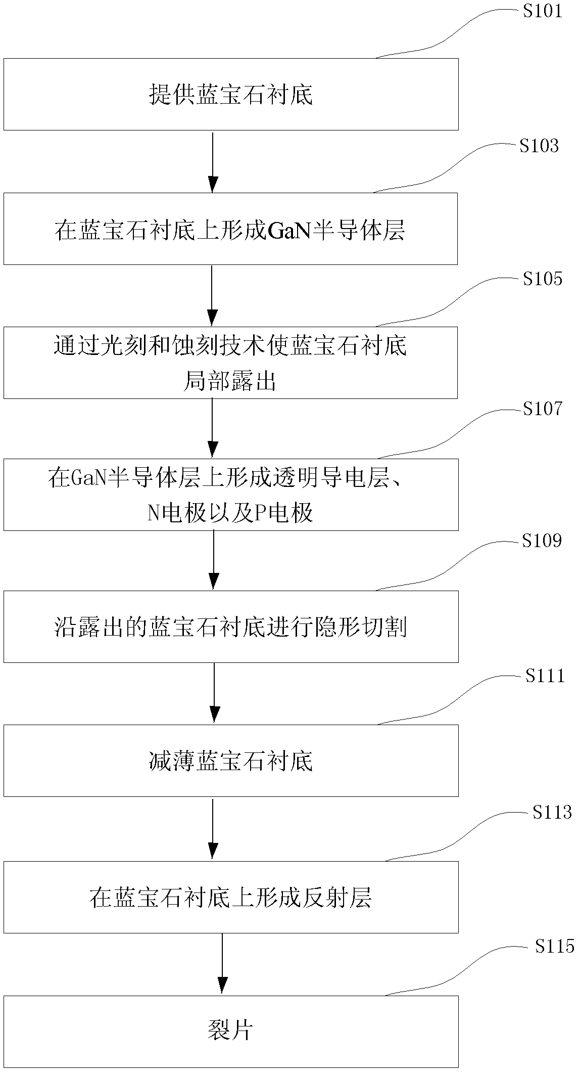
[0025] figure 1 It is a schematic flow chart of preparing a GaN-based LED chip according to the method for manufacturing a GaN-based LED chip according to Embodiment 1 of the present invention. Such as figure 1 Shown, described preparation method comprises the steps:

[0026] S101, providing a sapphire substrate;

[0027] S103, forming a GaN semiconductor layer on the sapphire substrate;

[0028] S105, partially exposing the sapphire substrate by photolithography and etching techniques;

[0029] S107, forming a transparent conductive layer, an N electrode and a P electrode on the GaN semiconductor layer;

[0030] S109, performing invisible cutting along the exposed sapphire substrate;

[0031] S111, thinning the sapphire substrate;

[0032] S113, forming a reflective layer on the sapphire substrate; and

[0033] S115, lobes.

[0034] The following combination Figure 1 to Figure 11 A method of manufacturing a GaN-based LED chip according to Embodiment 1 of the present i...

Embodiment approach 2

[0043] In Embodiment 1, step S105 is first performed, that is, the flat sapphire substrate 101 is partially exposed by photolithography and etching techniques, and then step S107 is performed to form a transparent conductive layer 106, an N electrode 107 and a P electrode 108 . In this embodiment, after forming the transparent conductive layer 106, the N electrode 107 and the P electrode 108 on the GaN semiconductor layer, the GaN semiconductor layer is etched by photolithography and etching techniques, so that the flat sapphire substrate 101 is locally Exposure is equivalent to exchanging the execution order of steps S105 and S107 in the first embodiment. The remaining parts are the same as those in Embodiment 1 and will not be repeated here.

Embodiment approach 3

[0045] In Embodiment 1, step S105 is first performed, that is, the flat sapphire substrate 101 is partially exposed by photolithography and etching techniques, and then step S107 is performed to form a transparent conductive layer 106, an N electrode 107 and a P electrode 108 . In this embodiment, the flat sapphire substrate 101 can be partially exposed during the formation of the transparent conductive layer 106, the N electrode 107 and the P electrode 108, or it can be formed after the transparent conductive layer 106 is formed, or after the N electrode 107 is formed. After that, or after the P electrode 108 is formed, the flat sapphire substrate 101 is partially exposed. The remaining parts are the same as those in Embodiment 1 and will not be repeated here.


PUM

PropertyMeasurementUnit
thicknessaaaaaaaaaa
wavelengthaaaaaaaaaa

Abstract

The invention provides a preparation method of a GaN-based LED (Light Emitting Diode) chip. The preparation method comprises the following steps of: 1) providing a sapphire substrate; 2) forming a GaN semiconductor layer on the front face of the sapphire substrate; 3) forming a transparent conductive layer, an electrode N and an electrode P; 4) thinning the sapphire substrate; 5) forming a reflective layer on the back face of the sapphire substrate; and 6) splitting the sheet and also comprises the following steps of: (a) locally exposing the sapphire substrate by using an photoetching and etching technology and (b) carrying out front face invisible cutting along the exposed sapphire substrate, wherein the step (a) is carried out prior to the step (b) and the steps (a) and (b) are respectively carried out behind the step 2) and before the step 4). According to the method provided by the invention, the advantages of the invisible cutting technology and the back face evaporation reflective layer technology can be brought into play at the same time; and obvious brightness increasing effect and stability effect, low production cost as well as simplicity and easiness in operation are obtained.

Description

technical field [0001] The invention relates to the field of preparation of semiconductor materials, in particular to a GaN-based light-emitting diode chip and a preparation method thereof. Background technique [0002] GaN-based light-emitting diodes (Light Emitting Diode, abbreviated as LED) have excellent characteristics such as long life, shock resistance, shock resistance, high efficiency and energy saving, and have extremely broad application prospects in image display, signal indication, lighting and basic research. GaN-based light-emitting diodes have developed rapidly in recent years, but their luminous efficiency has always been the main bottleneck restricting the wide application of LEDs in the lighting field. At present, the general process for preparing GaN-based LED chips is: 1) preparing a GaN semiconductor layer by epitaxial growth on a flat sapphire substrate or a patterned sapphire substrate (PSS for short); 2) on a GaN-based wafer Processing is carried ou...

Claims


Application Information

Patent Timeline
Patent Type & Authority Applications(China)
IPC IPC(8): H01L33/00H01L33/04H01L33/46
Inventor 陈诚郝茂盛张楠
Owner EPILIGHT TECH
Why Eureka
Try Eureka