Terahertz wave adjustable narrow band filter based on silicon-based photonic crystal structure
A photonic crystal and filter technology, applied in impedance networks, electrical components, multi-terminal-pair networks, etc., can solve the problems of narrow filter bandwidth, adjustable frequency range, harsh manufacturing process requirements, and complex modulation mechanisms, and achieve precise, fast and reliable performance. The effect of adjustment, absorption loss and low cost
- Summary
- Abstract
- Description
- Claims
- Application Information
AI Technical Summary
Problems solved by technology
Method used
Image
Examples
Embodiment 1
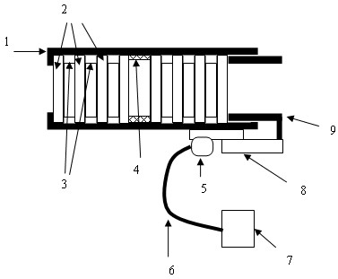
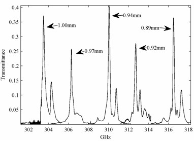
[0013] Embodiment 1: refer to figure 1 Schematic diagram, select a high-resistance silicon wafer with a thickness of 500μm±10μm (resistivity greater than 1000 ohm / cm) and cut it into a square piece of 2.2mm×2.2mm by a dicing machine; the ring piece is machined with a copper sheet of 0.6mm±0.2mm The inner hole is 1.9mm×1.9mm; the spring sheet is processed into a spring steel sheet with an inner hole of 1.9mm×1.9mm and an outer dimension of 2.2mm×2.2mm (unstressed length 1.2mm, minimum force length is 0.6). Put 6 square high-resistance silicon chips, ring-shaped copper sheets and a piece of spring alternately into the metal shell (inner size 2.3mm×2.3mm×20mm) to form a one-dimensional photonic crystal filter, put it into the aluminum square tube push column (2.2 mm×2.2mm×40mm), the outer end of the push column is fixed on the translation platform driven by the stepping motor through screws, and the metal tube and the base of the translation platform are fixed; the thickness of ...
Embodiment 2
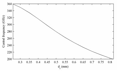
[0014] Example 2: Select a high-resistance silicon wafer with a thickness of 300 μm ± 5 μm (resistivity greater than 1000 ohms / cm), process a uniform square groove (groove depth about 200 μm) through an etching process, and use the square groove as the ring gasket 3, The silicon remaining at the bottom is a high-resistance silicon wafer 2 (2.2mm×2.2mm), forming a silicon wafer with a composite structure of a high-resistance silicon wafer and a ring gasket. The tunable filter is composed of six composite structure silicon chips and spring sheets, and its main working frequency bands are: 200GHz-360GHz, 520GHz-630GHz, 1THz-1.2THz, 1.85THz-2.02THz, etc., taking the 200GHz-360Ghz frequency band as an example, The transmittance of the filter center frequency is greater than 0.75, the filter bandwidth is about 300MHz, and the Q value is about 960. Figure 5 shows the relationship between the filter center frequency and the thickness of the defect.
PUM
 Abstract
Description
Claims
Application Information


