Device and method for removing glue from sample wafer

A sample and glue cavity technology, applied in the field of sample debonding devices, can solve the problems of loss of underlying silicon, damage to sensitive structures on the wafer surface, etc., to achieve no residue, mean square roughness and low silicon loss, and minimize the loss. Effect

Inactive Publication Date: 2012-02-01
INST OF MICROELECTRONICS CHINESE ACAD OF SCI
View PDF4 Cites 4 Cited by
  • Summary
  • Abstract
  • Description
  • Claims
  • Application Information

AI Technical Summary

Problems solved by technology

For the removal of implanted photoresist on silicon, alkaline or acidic fluorine-based solutions can be used, but it will cause loss of the underlying silicon; plasma removal technology can also be used, but the charge generated by the non-uniform plasma will damage the crystal. Sensitive structures on round surfaces

Method used


Image

  • Device and method for removing glue from sample wafer
  • Device and method for removing glue from sample wafer

Examples


Embodiment Construction

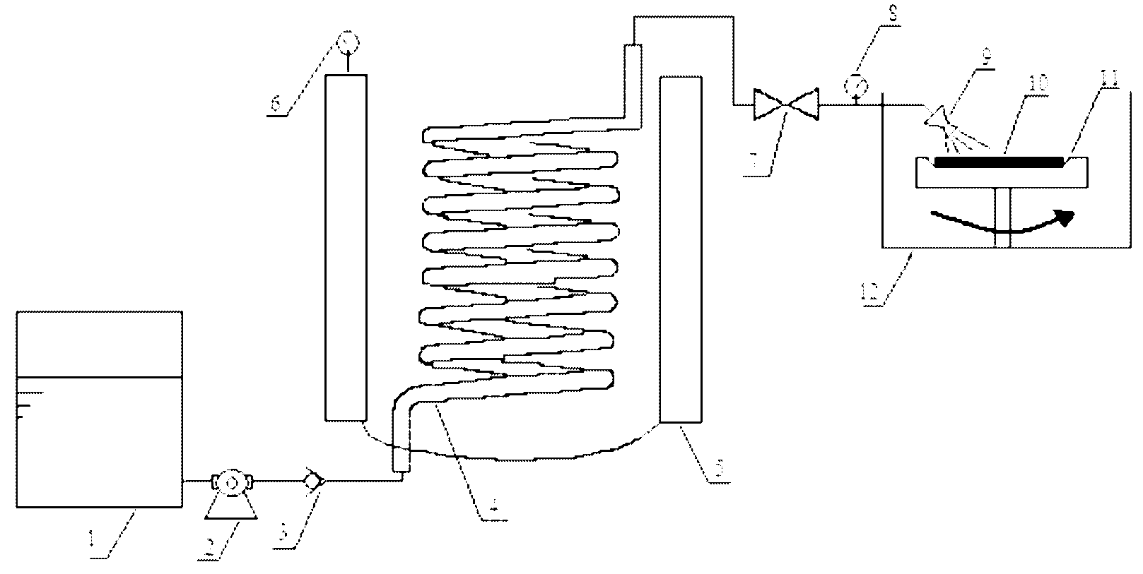
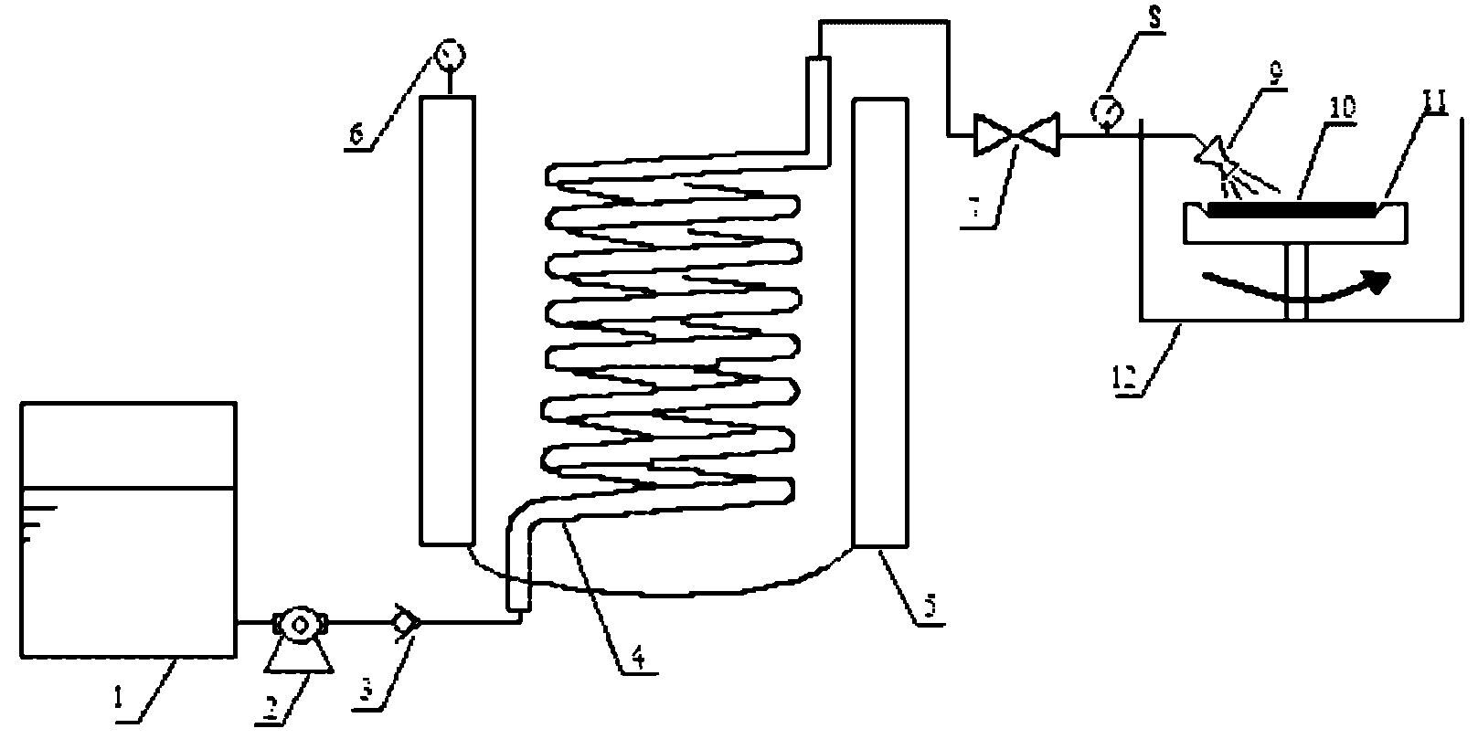
[0011] Such as figure 1 As shown, the sample stripping device provided by the embodiment of the present invention includes: a deionized water storage tank 1, a heat exchanger 4, a constant temperature heating device 5, a temperature display and control device 6, a glue removal chamber 12, and a nozzle 9. The outlet of the deionized water storage tank 1 is connected with a booster pump 2, and its outlet is connected to the inlet of the heat exchanger 4 through a one-way valve 3. The outlet of the heat exchanger 4 is connected to the inlet of the nozzle 9 via a valve 7. The heat exchanger 4 is made of Hastelloy, and the entire pipeline is coated with a fluorine coating. The constant temperature heating device 5 is made into a cylindrical cavity, and a heat exchanger 4 is arranged inside it. The thermostat heating device 5 is equipped with heat insulation materials outside. The heat exchanger 4 is fixed in the constant temperature heating device 5. A temperature control and di...


PUM


Abstract

The invention discloses a device for removing glue from a sample wafer. The device comprises a de-ionized water storage tank, a heat exchanger and a glue-removing chamber, wherein the de-ionized water storage tank is used for providing ultrapure de-ionized water; the heat exchanger is used for heating the ultrapure de-ionized water and causing the ultrapure de-ionized water to become a mixed fluid of water vapor and de-ionized water; the glue-removing chamber is used for removing the glue from the sample wafer by utilizing the mixed fluid; an outlet of the de-ionized water storage tank is connected to an inlet of the heat exchanger; and the outlet of the heat exchanger is connected to the inlet of the glue-removing chamber. The invention also provides a method for removing glue from the sample wafer. The method comprises the following steps of: forming the mixed fluid of water vapor and de-ionized water, and utilizing the mixed fluid to remove glue from the sample wafer. The method and device provided by the invention can be used for completely removing the organic optical resist and solidified optical resist from an inorganic carbonized thick layer and bottom. The glue-removing efficiency is high, no residue is left and the loss of a film material is minimized.

Description

Technical field [0001] The present invention relates to the field of semiconductor technology, in particular to a sample stripping device and method. Background technique [0002] In modern CMOS devices, almost all substrate structures are formed by ion implantation. High-energy ions can damage the photoresist, making it difficult to remove. After implantation, these ions will exist in the form of oxide layers, sub-oxide layers or organic compounds. These high-energy ions will also turn the surface of the photoresist into a carbonaceous layer of a mixture of diamond and graphite. Therefore, the carbonization process makes the removal of the implanted photoresist very challenging. For the removal of implanted photoresist on silicon, alkaline or acidic fluorine-based solutions can be used, but it will cause the loss of the underlying silicon; plasma removal technology can also be used, but the charge generated by the non-uniform plasma will damage the crystal Sensitive structur...

Claims


Application Information

Patent Timeline
Patent Type & Authority Applications(China)
IPC IPC(8): G03F7/32G03F7/30
Inventor 王磊景玉鹏
Owner INST OF MICROELECTRONICS CHINESE ACAD OF SCI
Why Eureka
Try Eureka