Micro-energy system with high energy density per unit volume and fabrication method thereof

A technology of micro-energy and specific energy, applied in the field of microelectronics, can solve the problems of low volume energy density, etc., and achieve the effect of increasing volume specific energy density, saving space, and reducing external circuit connections

Inactive Publication Date: 2012-02-08
SHANGHAI INST OF MICROSYSTEM & INFORMATION TECH CHINESE ACAD OF SCI
View PDF1 Cites 5 Cited by
  • Summary
  • Abstract
  • Description
  • Claims
  • Application Information

AI Technical Summary

Problems solved by technology

[0006] The purpose of the present invention is to provide a kind of micro-energy system with high volume specific energy density and its manufacturing method, which solves the problem of the low volume energy density of existing micro-energy systems (such as polymer lithium batteries, usually the volume energy density is only 100-200Wh / L) problem

Method used


Image

  • Micro-energy system with high energy density per unit volume and fabrication method thereof
  • Micro-energy system with high energy density per unit volume and fabrication method thereof
  • Micro-energy system with high energy density per unit volume and fabrication method thereof

Examples


Embodiment Construction

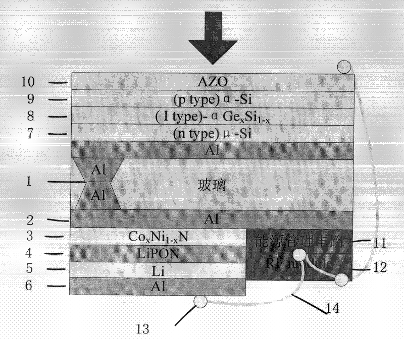
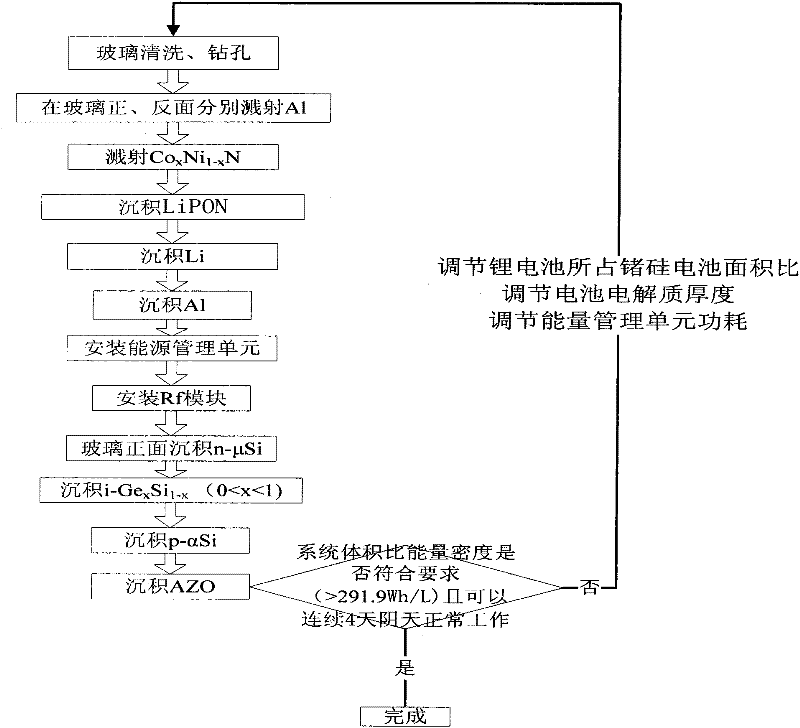
[0020] The manufacturing method of the high volume ratio energy density micro-energy system of the present invention, its manufacturing process (such as figure 2 )as follows:

[0021] 1. Drill holes on the glass substrate with a diamond drill, and the holes are two opposite hollow circular platforms (as shown in Figure 1).

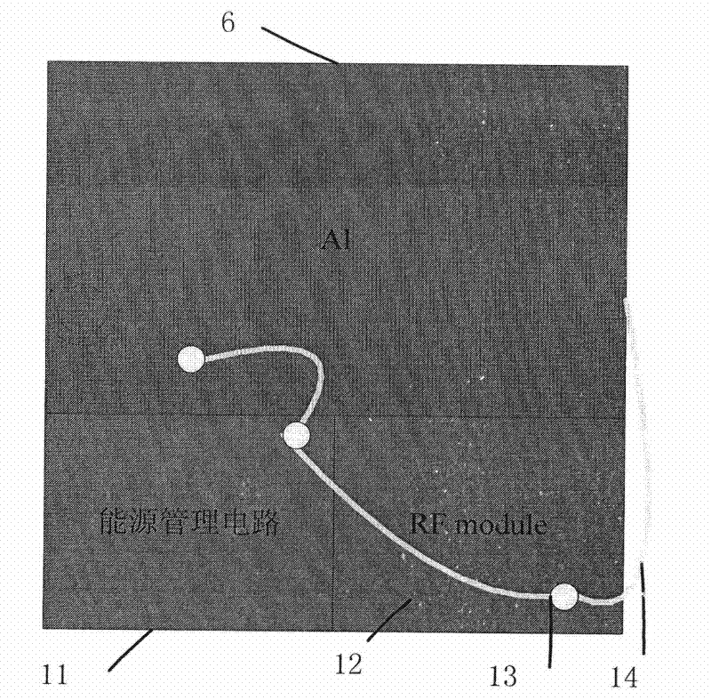
[0022] 2. Al films are sputtered on the front and back of the glass respectively, and the Al thickness is enough to fill the depth of the cavity to realize double-sided Al interconnection;

[0023] 3. Deposit cobalt nickel nitride, LiPON film, Li film and Al film on the back of Al in sequence; sputter deposit Co on the Al surface x Ni 1-x N, 0-4 Below Pa, the substrate temperature is less than 80°C during deposition until the thickness of the nickel-cobalt nitride film is 900nm; the LiPON film is deposited by sputtering on the surface of the nickel-cobalt nitride film; the LiPON film manufacturing process is to make Li 3 PO 4 Target, using this target,...


PUM

PropertyMeasurementUnit
thicknessaaaaaaaaaa
thicknessaaaaaaaaaa
thicknessaaaaaaaaaa

Abstract

The invention relates to a micro-energy system with high energy density per unit volume and a fabrication method thereof. The fabrication method of the system is characterized by comprising the following steps of: (a) drilling holes on a glass substrate by a diamond drill bit, wherein, the holes are two opposite hollow circular tables; (b) sputtering an Al membrane on the front face and rear face of the glass substrate so that the depth of a cavity is filled with the thickness of the Al membrane so as to realize double-sided Al interconnection; (c) sequentially depositing a cobalt-nickel nitride, a LiPON membrane, a Li membrane and an Al membrane on the rear face of Al; (d) arranging an energy management module and an RF (radio frequency) transceiver module on the surface of the Al membrane which is uncovered with a battery multilayer film; (e) sequentially depositing n-type microcrystalline silicon, i-type GexSi1-x (x is more than 0 and less than 1), p-type amorphous silicon and AZO containing 3% of Al on the Al surface of the front face of the glass substrate; and (f) connecting the AZO, a Li battery anode, an output end of the energy management module and an output end of the RF transceiver module by a Au line. In the invention, by adopting a sputtering deposit method, the energy density per unit volume of the obtained micro-energy system is more than 291.9W/L, which provides a technical means for node miniaturization of Internet of things, portability, long-time power supply and field application.

Description

technical field [0001] The present invention relates to a high volume specific energy density micro-energy system and a manufacturing method thereof, more specifically to a design of a high volume specific energy density micro-energy system that enables nodes of the Internet of Things to work normally under continuous cloudy conditions and preparation method. It belongs to the field of microelectronic technology. Background technique [0002] The miniaturization, distribution, and unattended sensor nodes of the Internet of Things are the future development trend. Special requirements are put forward for the volume, weight, power and working current of the energy source. There is an urgent need for small size, light weight, (volume ) micro energy source with high specific capacity to match it, and the monolithic integration of micro energy source and load will help to further improve the volume specific energy density of the micro system. [0003] Amorphous germanium silico...

Claims


Application Information

Patent Timeline
Patent Type & Authority Applications(China)
IPC IPC(8): H01M10/46H01M10/058
CPCY02E60/10Y02P70/50
Inventor 周健孙晓玮谈惠祖周舟周建华王伟刘正新
Owner SHANGHAI INST OF MICROSYSTEM & INFORMATION TECH CHINESE ACAD OF SCI
Why Eureka
Try Eureka