Tape base material for assembling display device, and adhesive sheet for assembling display device and display module unit using same
A technology of base materials and display devices, applied in the direction of film/sheet adhesives, applications, adhesives, etc., can solve problems such as incorrect operation of control devices, thicker adhesive tapes, and increased conductivity of light-shielding layers, and achieve Reduces electrical conductivity, excellent light-shielding properties, and prevents erroneous operations
- Summary
- Abstract
- Description
- Claims
- Application Information
AI Technical Summary
Problems solved by technology
Method used
Image
Examples
Embodiment 1
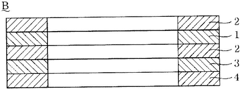
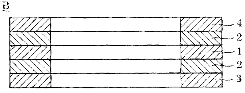
[0110] A colorless and transparent polyethylene terephthalate film (manufactured by Toray Co., Ltd., trade name “5AF53”) having a thickness of 4.5 μm was prepared as a transparent base material film 1 . It should be noted that the polyethylene terephthalate film does not contain any colored pigments. Moreover, corona discharge treatment was given to both surfaces of the transparent base film 1, and the surface tension of both surfaces of the transparent base film 1 was 50 mN / m.
[0111] A black ink (carbon black: 10% by weight) was prepared. The black ink consisted of 30 parts by weight of polyurethane resin (halogen element content: less than 50 ppm) as a binder, and the average particle diameter of a black colorant produced by a furnace method. It consists of 10 parts by weight of carbon black of 0.03 micrometers, and 60 parts by weight of the solvent which mixed ethyl acetate, toluene, and isopropanol.
[0112] A black ink was applied to one surface of the polyethylene ter...
Embodiment 2
[0118] Except that a light-shielding layer 2 with a thickness of 1 μm is formed on the two surfaces of the polyethylene terephthalate film 1 and is composed of a light-shielding base layer, the others are the same as in Example 1. Figure 4 Adhesive sheet B for display device assembly is shown.
Embodiment 3
[0120] The black ink was coated and dried on the light-shielding base layer integrated on one surface of the polyethylene terephthalate film 1, and this operation was performed once instead of repeating the above-mentioned operation in Example 1. 3 times to obtain the light-shielding base layer, forming a light-shielding layer with a thickness of 2 μm obtained by stacking and integrating two layers of light-shielding base layers. Except for this, the others are the same as in Example 1. Figure 4 Adhesive sheet B for display device assembly is shown.
PUM
| Property | Measurement | Unit |
|---|---|---|
| thickness | aaaaa | aaaaa |
| thickness | aaaaa | aaaaa |
| electrical resistance | aaaaa | aaaaa |
Abstract
Description
Claims
Application Information


