Small area electrically removing type rewritable read only memory array

A read-only memory and sub-memory technology, applied in the field of memory arrays, can solve problems such as increasing cost requirements and increasing area costs, and achieve the effect of reducing costs and reducing unit cell area

Active Publication Date: 2012-03-14
YIELD MICROELECTRONICS CORP
View PDF3 Cites 2 Cited by
  • Summary
  • Abstract
  • Description
  • Claims
  • Application Information

AI Technical Summary

Problems solved by technology

For the current non-volatile memory, its circuit diagram and circuit layout diagram are as follows figure 1 and figure 2 As shown, the non-volatile memory is a kind of memory composed of many storage cells. In the figure, each storage cell includes a transistor 10 and a capacitor structure 12, and the storage of every two adjacent one-byte groups There will be two bit lines between the unit cells, which will increase the area cost
and image 3 It is a cross-sectional view of the structure of each storage unit cell. It can be seen from the figure that the capacitor structure 12 is arranged on one side of the transistor 10. Due to such a structure, it will also cause a large area, thereby increasing the cost requirement.

Method used


Image

  • Small area electrically removing type rewritable read only memory array
  • Small area electrically removing type rewritable read only memory array
  • Small area electrically removing type rewritable read only memory array

Examples


Embodiment Construction

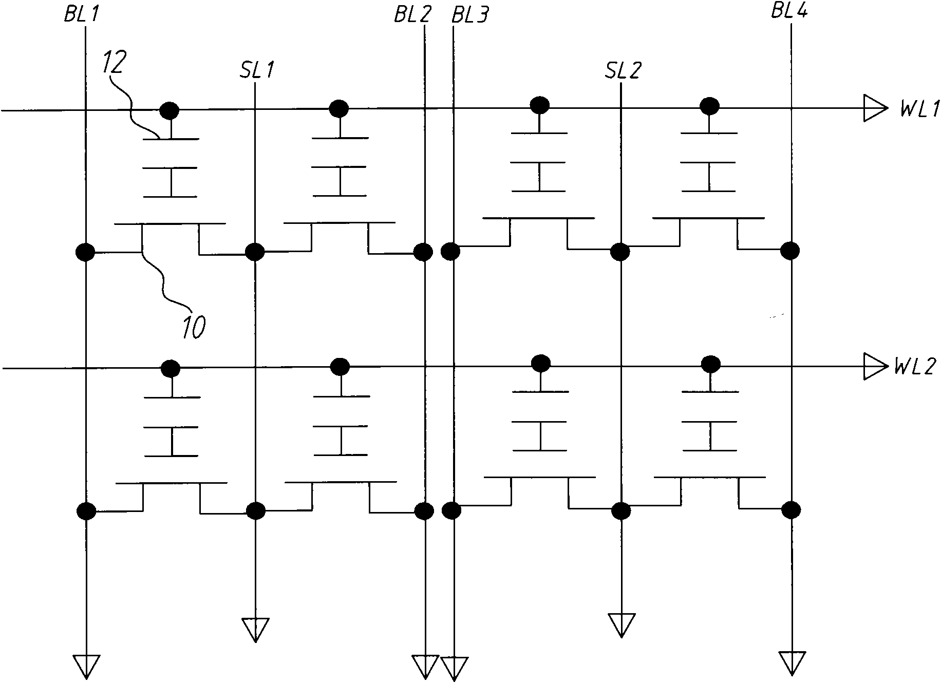
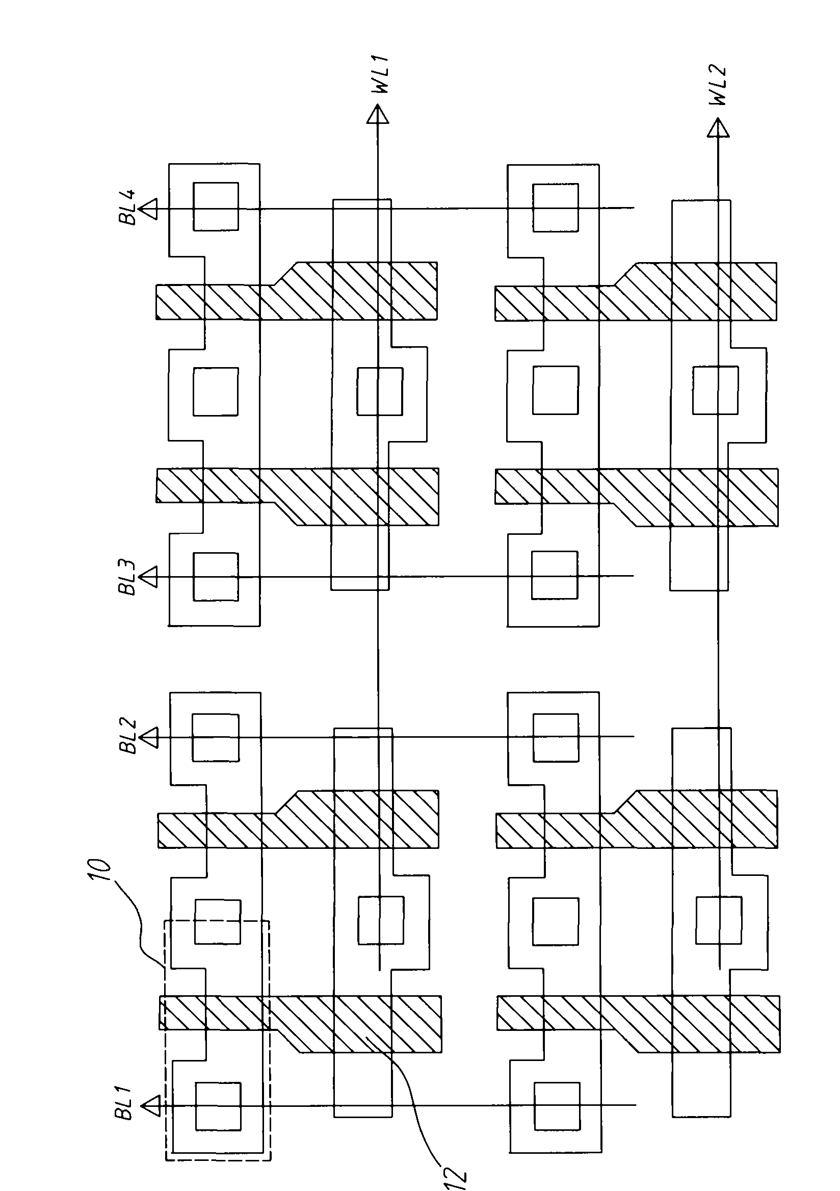
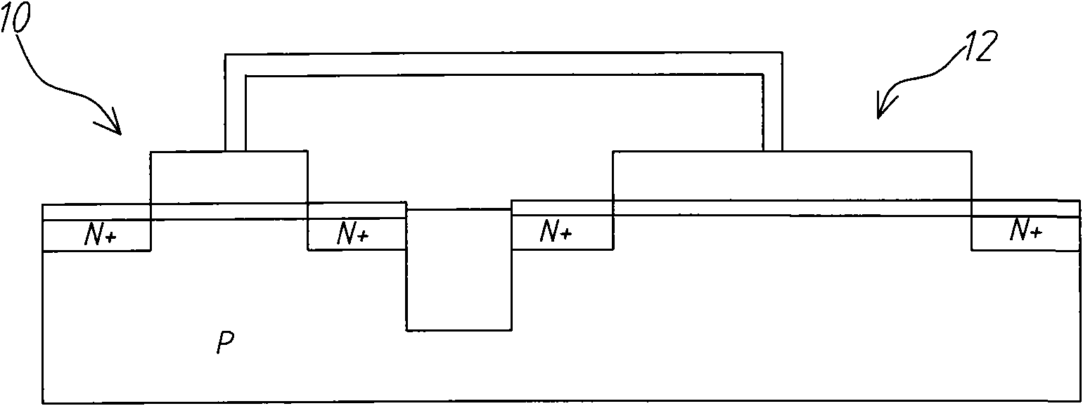
[0021] Please also refer to the following Figure 4 and Figure 5 , to introduce the first embodiment. The present invention includes a plurality of parallel bit lines 14, which are divided into multiple sets of bit lines 16, and the multiple sets of bit lines 16 include a first set of bit lines 18 and a second set of bit lines 19. One set of bit lines 18 and the second set of bit lines 19 both include a bit line 14 . There are also a plurality of parallel word lines 20 perpendicular to the bit line 14 , including a first word line 22 . There are a plurality of parallel common source lines 24 parallel to the word line 20 , including a first common source line 26 . The bit lines 14 , word lines 20 and common source lines 24 are connected to a multi-sub-memory array 28 , that is, 2×2 bit memory cells. Each sub-memory array 28 is connected to two sets of bit lines 16 , two word lines 20 and a common source line 24 , and each sub-memory array 28 is located between two adjacent...


PUM


Abstract

The invention provides a small area electrically removing type rewritable read only memory array which comprises a plurality of strips of parallel byte lines, word lines and common source lines. A plurality of strips of the byte lines are divided into a plurality of groups of byte lines which comprises a first group of byte lines and a second group of byte lines. The word lines comprise a first word line. The common source lines comprise a first common source line. The small area electrically removing type rewritable read only memory array also comprises a plurality of sub-memory arrays, eachsub-memory array comprises a first storage crystal cell, a second storage crystal cell, a third storage crystal cell and a fourth storage crystal cell which are connected with the two groups of byte lines, a word line and a common source line, wherein the first storage crystal cell and the second storage crystal cell are symmetrically provided, the third storage crystal cell and the fourth storage crystal cell are symmetrically provided, and the first storage crystal cell and the second storage crystal cell are in symmetric configuration with the third storage crystal cell and the fourth storage crystal cell respectively with the first common source line. According to the invention, area cost can be greatly reduced, and a byte write function is realized.

Description

technical field [0001] The invention relates to a memory array, in particular to a small-area electronic erasable rewritable read-only memory array. Background technique [0002] Complementary Metal Oxide Semiconductor (CMOS) process technology has become a common manufacturing method for application specific integrated circuits (ASIC). Today, with the development of computer information products, flash memory (Flash) and electronically erasable programmable read-only memory (Electrically Erasable Programmable Read Only Memory, EEPROM) both have non-volatile memory that can be programmed and erased electrically. Function, and the data will not disappear after the power is turned off, so it is widely used in electronic products. [0003] The non-volatile memory is programmable to store charge to change the gate voltage of the transistor of the memory, or not store charge to leave the gate voltage of the transistor of the original memory. The erasing operation is to remove t...

Claims


Application Information

Patent Timeline
Patent Type & Authority Applications(China)
IPC IPC(8): H01L27/115
Inventor 林信章戴家豪叶仰森杨明苍范雅婷
Owner YIELD MICROELECTRONICS CORP
Why Eureka
Try Eureka