Method and device for preparing silicon-based three-dimensional (3D) microstructure

A three-dimensional structure, silicon-based technology, used in the manufacture of microstructure devices, microstructure devices, microstructure technology, etc. Effect of surface quality, good aspect ratio

Inactive Publication Date: 2015-03-25
NANTONG UNIVERSITY
View PDF3 Cites 0 Cited by
  • Summary
  • Abstract
  • Description
  • Claims
  • Application Information

AI Technical Summary

Problems solved by technology

Whether it is wet etching or dry etching, it is difficult to produce microstructures with absolutely vertical sides, and the aspect ratio of microstructures is also limited.
[0004] In conclusion, so far, there is no method for the preparation of silicon-based micro-3D structures that has the advantages of low cost, simple process, large structure aspect ratio, good verticality, and high-quality processed surface.

Method used


Image

  • Method and device for preparing silicon-based three-dimensional (3D) microstructure
  • Method and device for preparing silicon-based three-dimensional (3D) microstructure
  • Method and device for preparing silicon-based three-dimensional (3D) microstructure

Examples


Embodiment Construction

[0028] The present invention will be described in further detail below in conjunction with the accompanying drawings and specific embodiments.

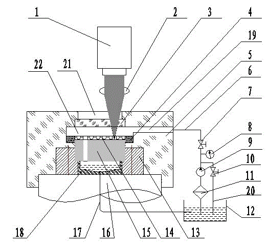
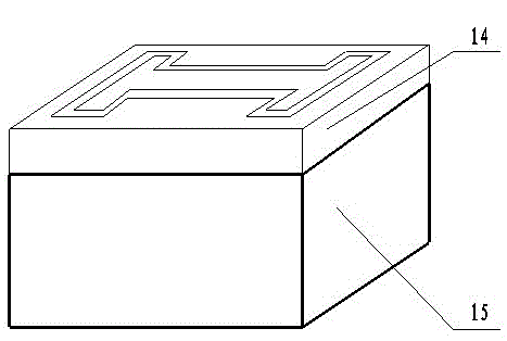
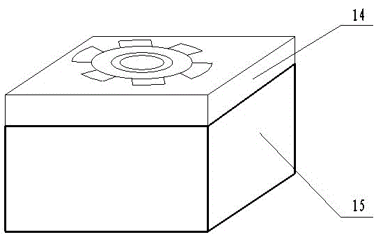
[0029] This example is in figure 2 Make the I-shaped micro-three-dimensional structure as shown on the pattern mask 14 on the silicon chip 15 shown, or as image 3 As shown, the tooth-shaped micro three-dimensional structure as shown on the pattern mask 14 is fabricated on the silicon wafer 15 .

[0030] Silicon wafers are in such figure 1 The setup shown is for the fabrication of micro-3D structures. The device is mainly composed of a laser 1, a focusing lens 2, a graphic mask 14, a work box 5, a workbench 16, a liquid collection tank 18 and a chemical solution circulation filtration system. Working box 5 upper end is provided with window 21, and the inboard of window 21 is provided with optical safety mirror 3, and window 21 below is a cavity 22, and one side of cavity 22 is provided with the liquid inlet cavity 19 that vertical...


PUM

PropertyMeasurementUnit
thicknessaaaaaaaaaa
wavelengthaaaaaaaaaa

Abstract

The invention relates to a method and a device for preparing a silicon-based three-dimensional (3D) microstructure. The method comprises the following steps: carrying out laser machining, chemical corrosion and combined machining on a silicon wafer covered with a picture mask; performing laser scanning and cutting along a preset track of the picture mask; simultaneously chemically etching a laser machining surface by utilizing a chemical solution; and finishing the machining surface. The device for implementing the method mainly consists of a laser, the picture mask, a focusing lens, a work box, a worktable, a liquid collecting tank and a chemical solution circulating and filtering system, wherein the work box is connected on the worktable, a cavity is arranged inside the work box, and a window is arranged on one end of the work box; the picture mask is adhered to the upper end face of the silicon wafer and is placed in the cavity; the liquid collecting tank is placed below the silicon wafer; the chemical solution circulating and filtering system is communicated with the cavity and the liquid collecting tank; the focusing lens and the laser are placed at one side of the window; and lasers are focused on the silicon wafer through the focusing lens and the window. The silicon-based 3D microstructure obtained by the method has the advantages of large height-width ratio, good perpendicularity and good surface quality.

Description

technical field [0001] The invention relates to a method for manufacturing a silicon-based micro three-dimensional structure, and specifically relates to the production of a silicon-based micro three-dimensional structure and a corresponding processing device by using laser action and chemical action in conjunction with a graphic mask. Background technique [0002] Due to the good electronic and mechanical properties of silicon-based materials, they are widely used in MEMS such as integrated circuits, micro-sensors, and micro-actuators. [0003] Silicon-based materials are not easy to process, and the typical processing methods of silicon-based micro three-dimensional structures include wet etching and dry etching. Wet etching refers to the chemical or electrochemical etching of silicon with chemical reagent solution; dry etching refers to the bombardment etching of silicon with high-energy ions or reactive gases under high vacuum conditions, such as plasma and reactive ion ...

Claims


Application Information

Patent Timeline
Patent Type & Authority Patents(China)
IPC IPC(8): B81C1/00
Inventor 张华花国然王强
Owner NANTONG UNIVERSITY
Why Eureka
Try Eureka