Probe card and manufacture method

A manufacturing method and probe card technology, applied in the manufacture of measuring instruments, measuring devices, instruments, etc., can solve problems such as poor contact of pads, indentation of pads, affecting test reliability and accuracy, and achieve low production costs , the effect of reducing the arrangement density

Inactive Publication Date: 2012-03-21
ADVANCED SEMICON ENG INC
View PDF9 Cites 8 Cited by
  • Summary
  • Abstract
  • Description
  • Claims
  • Application Information

AI Technical Summary

Problems solved by technology

[0004] The probe card contains a plurality of precision probes, that is, the tip of each probe is fine-pitched (substantially less than 100 microns), and due to the influence of manufacturing process parameter variations, these probes are Under normal circumstances, the relative positioning and flatness will have too large deviation, which will cause poor contact or excessive indentation on the pad of the object under test, which will affect the reliability and accuracy of the test.
[0005] In addition, the distance between these probes of various existing probe cards cannot be reduced, so that electrical testing of fine-pitch contacts cannot be performed, and the types of chips that can be tested are limited.

Method used


Image

  • Probe card and manufacture method
  • Probe card and manufacture method
  • Probe card and manufacture method

Examples


Embodiment Construction

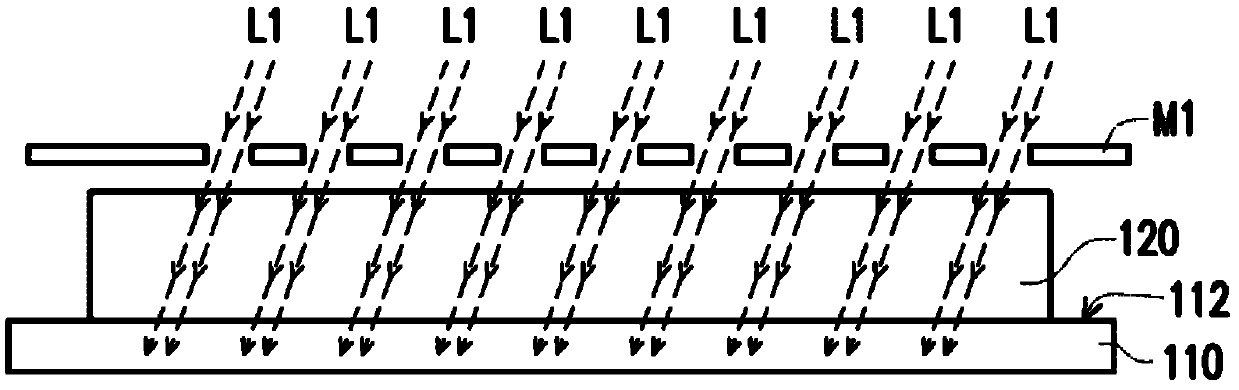
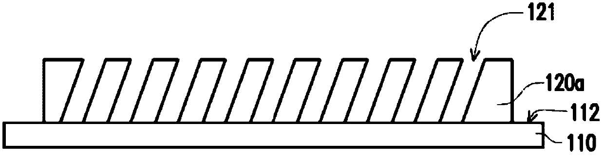
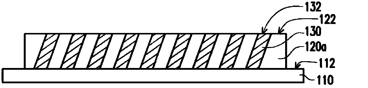
[0046] Figure 1A to Figure 1H It is a schematic cross-sectional view of a method for manufacturing a probe card according to an embodiment of the present invention. According to the manufacturing method of the probe card of this embodiment, at first, please refer to Figure 1A , providing a carrier 110, wherein the carrier 110 has an upper surface 112, and a first photoresist layer 120 has been coated on the upper surface 112. In this embodiment, the carrier 110 is, for example, a silicon circuit substrate or a resin (such as bismaleimide-triazineresin (BT resin)) circuit substrate. That is to say, the carrier 110 is a silicon substrate or a BT substrate with a circuit structure (not shown). The carrier 110 can also be a flexible substrate.

[0047] Next, please also refer to the Figure 1A and Figure 1B , providing a first patterned photomask M1, and obliquely exposing the first photoresist layer 120 in a first exposure direction L1 to form a first patterned photoresis...


PUM


Abstract

The present invention discloses a rpobe card and a manufacture method, wherien the probe card comprises a carrier and a plurality of probes, the carrier is provided with an upper surface, the probes are configured on the carrier and arranged on the upper surface, each probe is provided with atleast serially connected first and second rod body portions, the first rod body portion is arranged on the upper surface and form a slant angle together with the upper surface, and between the extending directions of the first rod body portion and the second rod body portion there is provided an included angle.

Description

technical field [0001] The invention relates to a test element and its manufacturing method, and in particular to a probe card capable of maintaining relative positioning and flatness of probes and its manufacturing method. Background technique [0002] Electrical testing of an integrated circuit chip (IC chip) is very important in the manufacturing process. Each IC chip must be tested in wafer and package form to ensure its electrical function. When the integrated circuit is tested, the testing machine contacts the device under test (DUT) through a probe card, and transmits the electrical signal through the driving signal, and then analyzes the received electrical signal to obtain that the integrated circuit under test is a good product or The result of waste. [0003] When individual chips are tested in wafer form, the process is called wafer testing. The method of wafer detection is to make the test machine and the probe card form a test circuit, and directly contact t...

Claims


Application Information

Patent Timeline
Patent Type & Authority Applications(China)
IPC IPC(8): G01R1/073G01R3/00
Inventor 陈明坤朱伟硕蔡昭源
Owner ADVANCED SEMICON ENG INC
Why Eureka
Try Eureka