Method for forming semiconductor device with metal grid electrode

A metal gate and semiconductor technology, applied in semiconductor devices, semiconductor/solid-state device manufacturing, electric solid-state devices, etc., can solve problems that affect the reliability of semiconductor devices, aggravate short-channel effects, reduce overall performance, etc., and achieve improved short-circuit The effect of channeling effect, ensuring reliability and improving yield rate

Inactive Publication Date: 2012-03-21
SEMICON MFG INT (SHANGHAI) CORP +1
View PDF5 Cites 0 Cited by
  • Summary
  • Abstract
  • Description
  • Claims
  • Application Information

AI Technical Summary

Problems solved by technology

[0007] However, semiconductor devices with metal gates formed by this traditional method have high gate-induced leakage current (GIDL), which affects the reliability of semiconductor devices and reduces their overall performance
The traditional solution to the problem of excessively high GIDL is to reduce the concentration of channel doping, but this will aggravate the problem of short channel effect

Method used


Image

  • Method for forming semiconductor device with metal grid electrode
  • Method for forming semiconductor device with metal grid electrode
  • Method for forming semiconductor device with metal grid electrode

Examples


Embodiment Construction

[0024] In the following description, a lot of specific details are given in order to provide a more thorough understanding of the present invention. However, it is obvious to those skilled in the art that the present invention can be implemented without one or more of these details. In other examples, in order to avoid confusion with the present invention, some technical features known in the art are not described.

[0025] In order to thoroughly understand the present invention, detailed steps will be presented in the following description to illustrate how the present invention forms a semiconductor device with a metal gate. Obviously, the implementation of the present invention is not limited to the specific details familiar to those skilled in the semiconductor field. The preferred embodiments of the present invention are described in detail as follows. However, in addition to these detailed descriptions, the present invention may also have other embodiments.
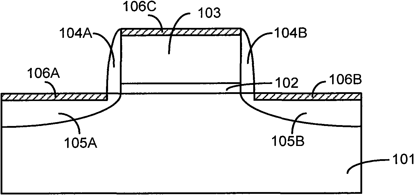
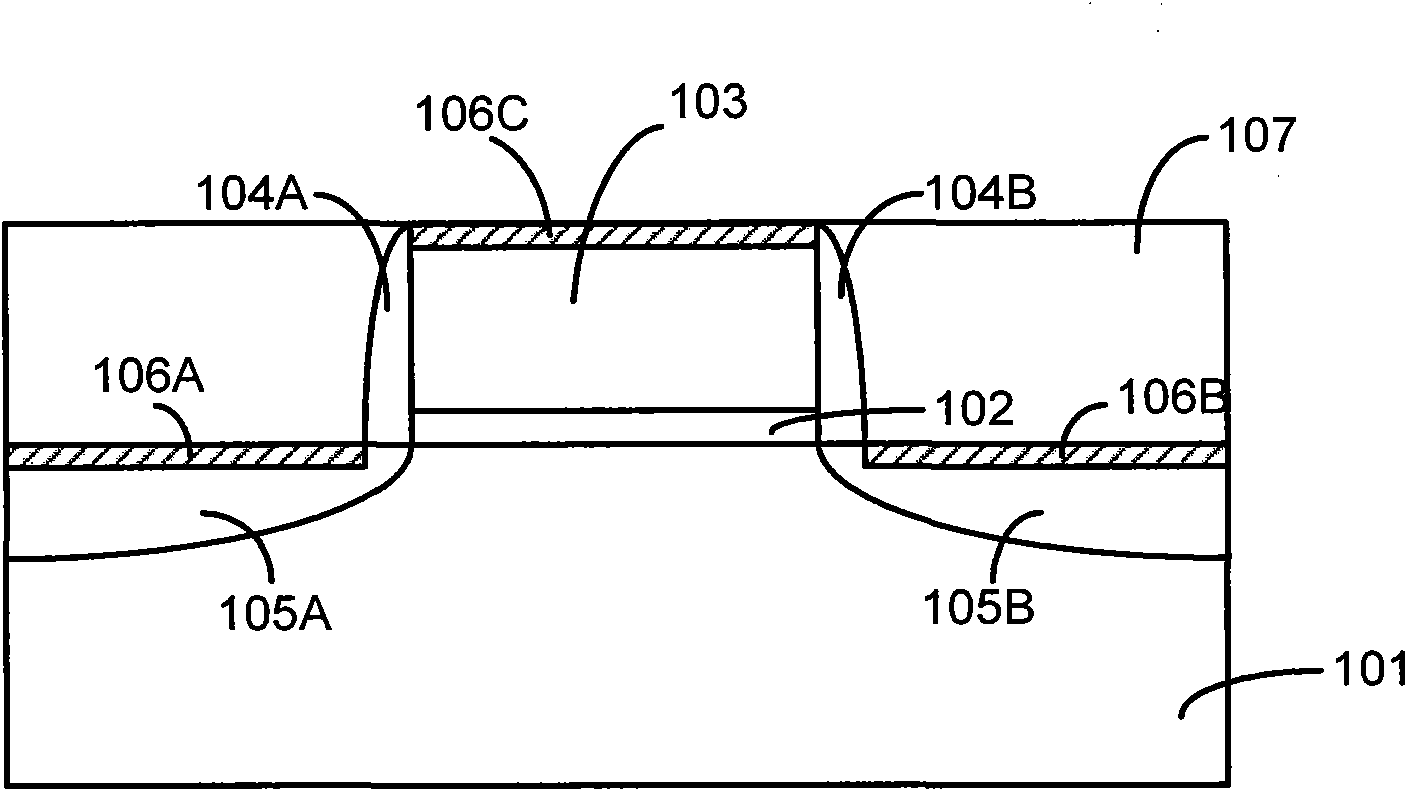
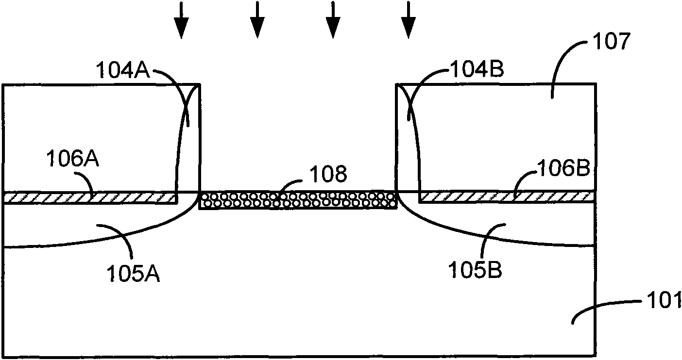
[0026] Refer t...


PUM


Abstract

The invention provides a method for forming a semiconductor device with a metal grid electrode, which comprises the steps of: providing a front-end device structure, wherein the front-end device structure is provided with a semiconductor substrate and an interlayer medium layer arranged on the semiconductor substrate, the interlayer medium layer is internally provided with an opening from which a part of the semiconductor substrate is exposed, and the semiconductor substrate which is arranged at two sides of the opening and is covered by the interlayer medium layer is internally provided with a source electrode / a drain electrode; forming a barrier layer on the front-end device structure; etching the barrier layer, so that a barrier gap wall layer is formed on the side wall of the opening; performing an ion implantation technology to the semiconductor substrate by the means that the barrier gap wall layer and the interlayer medium layer are taken as mask films, so that an unevenly-doped channel is formed; removing the barrier gap wall layer; and forming a high-k material layer in the opening, and filling with metal, so that the semiconductor device with the metal grid electrode is formed. After the semiconductor device with the metal grid electrode is formed according to the method provided by the invention, not only can the gate induced drain leakage (GIDL) be effectively reduced, but also the short channel effect can be improved.

Description

Technical field [0001] The present invention relates to a semiconductor manufacturing process, in particular to a method of forming a semiconductor device with a metal gate. Background technique [0002] With the rapid development of microelectronics technology, CMOS technology, the core of microelectronics technology, has become the supporting technology in modern electronic products. For decades, chip manufacturers have consistently adopted silicon dioxide (SiO 2 ) As the gate dielectric layer and using doped polysilicon as the gate electrode material. This combination continues until the 90-nanometer node era. As the critical size (CD) continues to shrink, the SiO in CMOS transistors 2 The size of the gate dielectric layer has reached its limit. For example, when using the 65nm node process, SiO 2 The height of the gate dielectric layer has been reduced to 1.2 nanometers, which is about the height of 5 silicon atomic layers. If it is further reduced, the leakage current and ...

Claims


Application Information

Patent Timeline
IPC IPC(8): H01L21/8238H01L21/28H01L27/105
Inventor 刘金华
Owner SEMICON MFG INT (SHANGHAI) CORP
Why Eureka
Try Eureka