Gallium element doping device and method for Czochralski silicon
A technology of element doping and Czochralski silicon, which is applied in the field of doping devices, can solve the problems of difficulty, difficult secondary doping, high cost, etc., to reduce the temperature stabilization time, make the doping device simple and practical, and improve production efficiency effect
- Summary
- Abstract
- Description
- Claims
- Application Information
AI Technical Summary
Problems solved by technology
Method used
Image
Examples
Embodiment 1
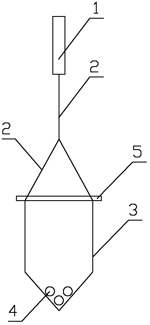
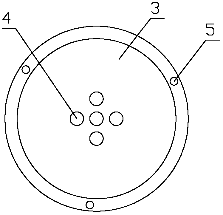
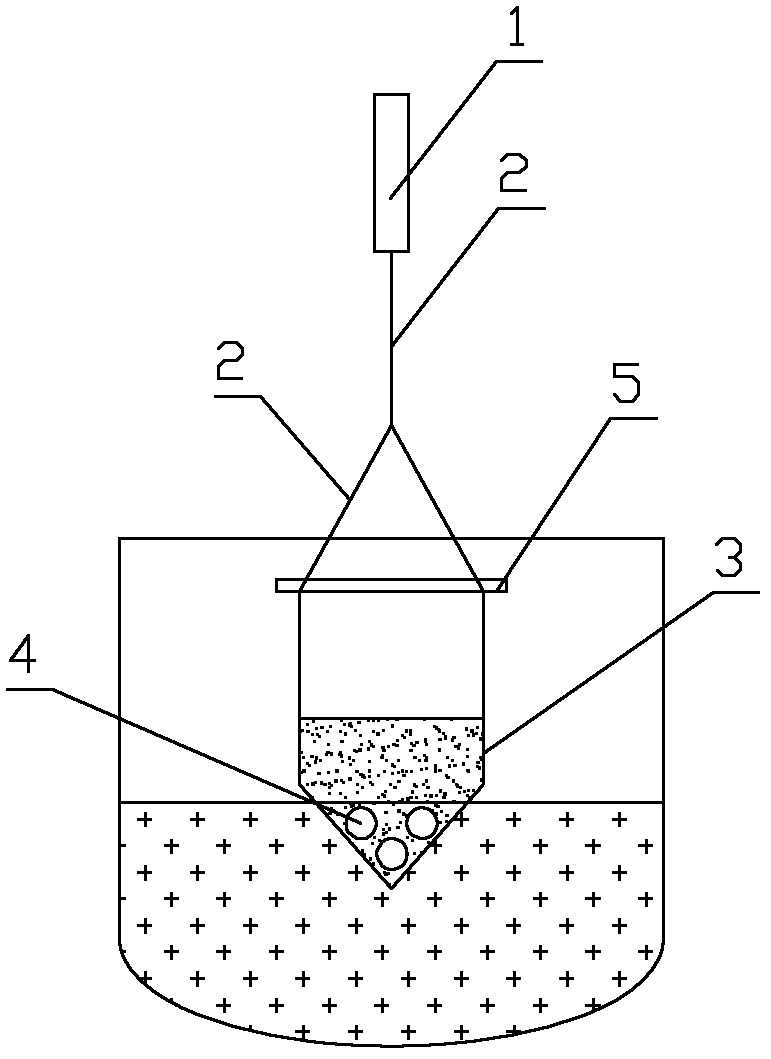
[0038] Embodiment 1, the method of using the device: ① After the polysilicon in the single crystal furnace is completely melted; ② Use the gate valve of the single crystal furnace to isolate the auxiliary room of the main room; ③ Open the auxiliary room, remove the seed crystal, and install the device. During the whole process, pay attention to ensure cleanliness and prevent contamination; ④Put gallium metal into the doping cup; ⑤Clean the sub-chamber and connect it to the main chamber and sub-chamber, lower the doping device and enter the liquid surface 8mm; , the dopant completely flows into the melt; ⑦lift the device, the doped hole is re-sealed by the adsorbed molten silicon, and the device is lifted into the auxiliary chamber; ⑧The gate valve isolates the main chamber and the auxiliary chamber, and the auxiliary chamber Inflate the chamber to normal pressure, open the door of the auxiliary chamber, and after cooling for a certain period of time, remove the device, reinstal...
Embodiment 2
[0039]Example 2, the equipment is a TDR-80 single crystal furnace, the initial polysilicon feeding amount is 60Kg, the crystal diameter is 170 mm, the target resistivity is 2 ohm cm, and 300 mg of gallium metal is weighed, and the doping device is used for doping. The specific implementation is as follows Example 1 is carried out, and the total time of the whole doping process is 35min. After the melt is stable, place a suitable crucible for the steps of seeding, laying shoulders, turning shoulders, equal diameter, and finishing. About 2.15 ohm cm, tail resistivity 0.96 ohm cm. It basically meets the requirements of the target resistivity of the head, and the deviation from the target resistance is only 7.5%.
Embodiment 3
[0040] Example 3, secondary supplementary doping of solar energy, due to equipment reasons or process control reasons, the primary isocrystalline length is 326 mm, and the secondary isomorphic diameter is 180 mm. Due to the loss of dislocation-free growth state, the high temperature remelts twice, and the total weight of the lifting shoulder is 1.2kg. In order to ensure that the resistivity of the crystal is within the target resistivity of 2.1 ohm cm, the doping concentration of the melt is recalculated and 70 mg of dopant is added. Use the above gallium-doped device, and perform supplementary doping according to the method of Example 1. After the doping is completed, the crystal is grown according to the normal process, with an equal diameter of 1000mm, and the head and tail samples are taken for resistivity testing, and the target resistivity deviation is less than 5%.
[0041] The main principle of the present invention is as follows: the present invention utilizes the su...
PUM
| Property | Measurement | Unit |
|---|---|---|
| diameter | aaaaa | aaaaa |
| height | aaaaa | aaaaa |
Abstract
Description
Claims
Application Information


