Manufacture method of through hole of large size

A manufacturing method and large-scale technology, applied in semiconductor/solid-state device manufacturing, electrical components, circuits, etc., can solve problems such as difficulty in achieving a sufficient thickness of the barrier layer, and achieve the effect of a simple process method

Inactive Publication Date: 2012-04-11
SHANGHAI HUAHONG GRACE SEMICON MFG CORP
View PDF3 Cites 9 Cited by
  • Summary
  • Abstract
  • Description
  • Claims
  • Application Information

AI Technical Summary

Problems solved by technology

[0005] The technical problem to be solved by the present invention is to provide a method for manufacturing large-sized through holes. This method solves the problem that it is difficult to achieve a suffici

Method used


Image

  • Manufacture method of through hole of large size
  • Manufacture method of through hole of large size
  • Manufacture method of through hole of large size

Examples


Embodiment Construction

[0023] The present invention will be described in further detail below in conjunction with the accompanying drawings and embodiments.

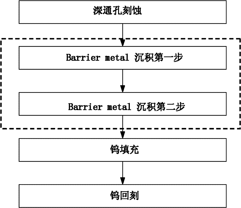
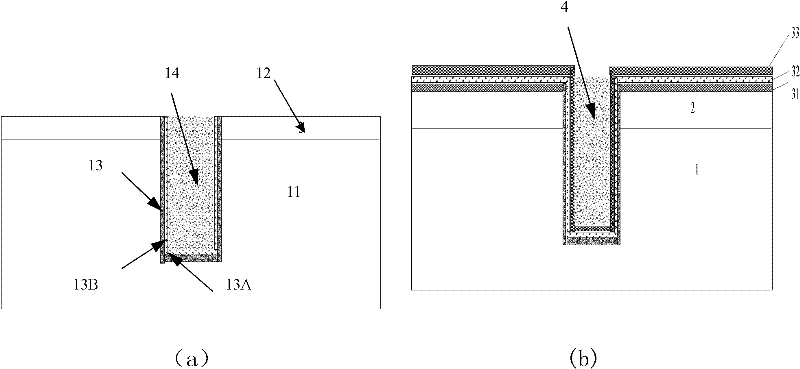
[0024] The invention provides a novel method for making large-sized through holes. After the through holes are etched, two different processes are used to deposit the barrier layer metal. First, MOCVD (Metal Organic Chemical Vapor Deposition) is used to deposit metal with good steps. The Ti / TiN film with covering ability can block the erosion (attack) on the side wall and bottom of the hole during the tungsten deposition process, and then use PVD (physical vapor deposition) method to deposit a certain thickness of TiN as the silicon surface for subsequent tungsten back etching barrier layer. In this way, both the electrical performance of the deep hole and the corresponding process control can be taken into account.

[0025] The manufacturing method of a kind of novel large-size through-hole of the present invention, its specific technologica...


PUM

PropertyMeasurementUnit
Thicknessaaaaaaaaaa

Abstract

The invention discloses a manufacture method of a through hole of large size. The method comprises the following steps of: (1) etching a deep through hole; (2) forming a first layer of barrier layer metal through a first step of barrier layer metal deposit, wherein a Ti/TiN double layer or a single TiN layer is adopted; (3) forming a second layer of barrier layer metal through a second step of barrier layer metal deposit, wherein a single TiN layer is adopted; (4) filling the deep through hole with tungsten; and (5) carrying out tungsten etch-back. in the invention, two steps of different processes are adopted to deposit the barrier layer metal, namely, firstly, a Ti/TiN film with good step covering capability is deposited by MOCVD (Metal Organic Chemical Vapor Deposition Equipment), and etching to side walls and the bottom of the through hole is prevented during tungsten deposit; secondly, a TiN layer of certain depth is deposited by a method of PVD (Physical Vapor Deposition) and the TiN layer serves as a surface barrier layer of later tungsten etch-back. As a result, the electric performance and corresponding process control of the deep through hole can both ensured.

Description

technical field [0001] The invention belongs to the manufacturing process of semiconductor integrated circuits, in particular to a method for manufacturing large-size through holes. Background technique [0002] In the back-end-of-line (BEOL) process of integrated circuits or discrete devices above 0.35um (microns), via holes are usually used to realize the connection between the gate and the metal layer or interlayer metal. Usually the diameter of the through hole is about 20-50nm. However, in some discrete devices such as RFLDMOS (radio frequency power circuit) or SiGe BiCMOS (silicon germanium bipolar CMOS, composed of bipolar gate circuit and complementary metal oxide semiconductor gate circuit, the bipolar process and CMOS process are compatible) process will be Some trench-type deep via structures are used to directly connect with the source or buried layer of the silicon substrate to reduce the on-resistance of the device and improve the frequency characteristics. I...

Claims


Application Information

Patent Timeline
IPC IPC(8): H01L21/768H01L21/3205
Inventor 程晓华彭虎
Owner SHANGHAI HUAHONG GRACE SEMICON MFG CORP
Why Eureka
Try Eureka