White light-emitting diode (LED) epitaxial structure and manufacturing method thereof, and white LED chip structure
A technology of LED chip and epitaxial structure, which is applied in the direction of electrical components, circuits, semiconductor devices, etc., and can solve the problems of poor color rendering, blue light spots, and scattering and absorption of white light LEDs
- Summary
- Abstract
- Description
- Claims
- Application Information
AI Technical Summary
Problems solved by technology
Method used
Image
Examples
Embodiment Construction
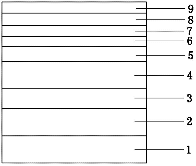
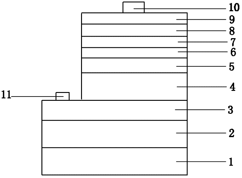
[0028] Such as figure 1 As shown, a white light LED epitaxial structure includes an epitaxial wafer, and the epitaxial wafer includes a ZnS substrate 1, a GaN transition layer 2, a first N-GaN contact layer 3, a Si- and Zn-doped In 0.2 Ga 0.8 N / GaN multi-quantum well light-emitting layer 4, first P-GaN contact layer 5, N-GaN cascade layer 6, second N-GaN contact layer 7, In doped with Si and Zn 0.49 Ga 0.51 N / GaN multi-quantum well light-emitting layer 8 and the second P-GaN contact layer 9 . The ZnS substrate is a nanoscale material with wide energy band gap, high refractive index and high light transmittance, and has excellent fluorescence effect and electroluminescence function.
[0029] Wherein, the thickness of the ZnS substrate 1 is 50-200um, preferably 100um.
[0030] Wherein, the thickness of the GaN transition layer 2 is 10-100 nm, preferably 50 nm.
[0031] Wherein, the thicknesses of the first N-GaN contact layer 3 and the second N-GaN contact layer 7 are both...
PUM
 Abstract
Description
Claims
Application Information
 - R&D Engineer
- R&D Manager
- IP Professional
- Industry Leading Data Capabilities
- Powerful AI technology
- Patent DNA Extraction
Browse by: Latest US Patents, China's latest patents, Technical Efficacy Thesaurus, Application Domain, Technology Topic, Popular Technical Reports.
© 2024 PatSnap. All rights reserved.Legal|Privacy policy|Modern Slavery Act Transparency Statement|Sitemap|About US| Contact US: help@patsnap.com


