

SRAM (Static Random Access Memory) unit structure based on fake contact etch stop layer technology and preparation method of SRAM unit structure
A technology of through-hole etching and cell structure, applied in electrical components, semiconductor/solid-state device manufacturing, electrical solid-state devices, etc., can solve the problems of non-contribution, static noise redundancy, etc. Large static noise redundancy, the effect of improving performance
- Summary
- Abstract
- Description
- Claims
- Application Information
AI Technical Summary
Problems solved by technology
Method used
Image

Examples
Embodiment Construction
[0024] The specific embodiment of the present invention will be further described below in conjunction with accompanying drawing:
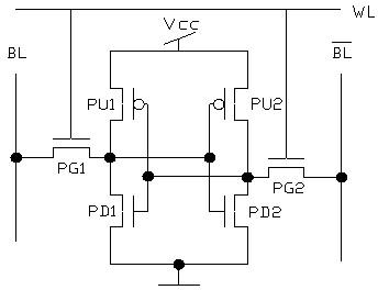
[0025] Figure 5 It is a structural schematic diagram of the structure of each semiconductor device of the static random access memory unit and its manufacturing method based on the pseudo-via etch stop layer (CESL, Contact etch stop layer) technology of the present invention, please refer to Figure 5 , a static random access memory cell structure based on pseudo-via etching stop layer technology and a manufacturing method thereof, wherein, in the production process of the static random access memory cell, on the pull-down transistor (Pull Down NMOS) Covering the tensile stress film (Tensile liner), and covering the compressive stress film (Compressive liner) on the pull-up transistor (Pull Up PMOS) and the pass transistor (Passing Gate NMOS), the existing technology is only from the perspective of improving device performance Start by covering ...
PUM
 Abstract
Description
Claims
Application Information