Organic field effect transistor with dielectric modification layer and preparation method thereof

An organic field and transistor technology, which is applied in the field of organic field effect transistors and its preparation, can solve the problems of shortage, uncertainty of the number of hydroxyl groups on the surface of the dielectric layer, uneven distribution, etc., achieve a small threshold voltage, and overcome the uncertainty of bonding The effect of sex and distribution inhomogeneity

Inactive Publication Date: 2013-07-03
UNIV OF SCI & TECH BEIJING
View PDF2 Cites 0 Cited by
  • Summary
  • Abstract
  • Description
  • Claims
  • Application Information

AI Technical Summary

Problems solved by technology

[0005] The purpose of the present invention is to overcome the surface hydroxyl group of the dielectric material layer in the existing dielectric layer modification method to be introduced through the method of hydrophilic treatment, resulting in the uncertainty of the number of hydroxyl groups on the surface of the dielectric layer and the inhomogeneity of distribution, and then affecting To solve the problem of insufficient performance of the final device, a method for using a zinc compound as an interface modification layer of an organic semiconductor / dielectric layer is provided, through the introduction of the modification layer, the carrier mobility of the organic field effect transistor is improved and the device is simultaneously endowed with New function (i.e. photoresponse function)

Method used


Image

  • Organic field effect transistor with dielectric modification layer and preparation method thereof
  • Organic field effect transistor with dielectric modification layer and preparation method thereof

Examples


Embodiment 1

[0035] Implementation steps:

[0036] Step 1: Cleaning of Silicon Substrate

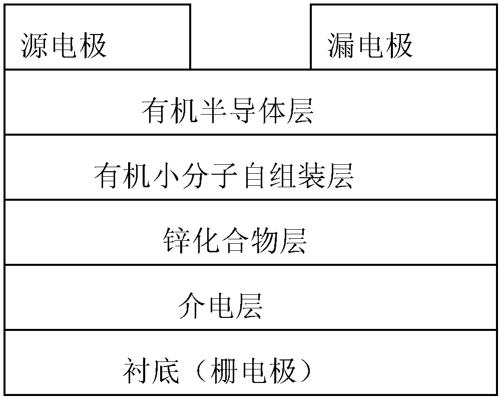
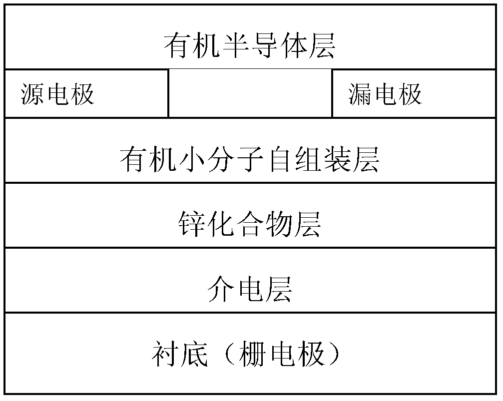
[0037] will have SiO 2 (thickness is 303 nanometers) n-type heavily doped silicon substrate (resistivity 0.02—0.04Ωcm) of the dielectric layer is ultrasonically cleaned with detergent, tap water, deionized water, acetone, and absolute ethanol for 5 minutes, and then placed Dry in oven.

[0038] Step 2: Deposition of Zinc Compound Layer

[0039] Spin-coat a solution of diethylzinc in cyclohexanone (concentration: 0.01 M) on the above-mentioned silicon substrate, so that the SiO 2 A zinc compound layer is formed on the surface with a thickness of 30 nm.

[0040] The third step: annealing treatment of the zinc compound layer

[0041] The silicon wafer deposited with the zinc compound was placed in an oven, and annealed at 180° C. for 15 minutes in the atmosphere.

[0042] Step 4: Deposition of organic small molecule self-assembled layer

[0043] OTMOS trichlorethylene solution (concentration: 3 m...

Embodiment 2

[0055] The device was prepared according to the method of Example 1, except that poly(3-hexylthiophene) was selected as the organic semiconductor material.


PUM


Abstract

The invention relates to an organic field effect transistor with a dielectric modification layer, which belongs to the field of organic semiconductor devices and is characterized in that the organic field effect transistor comprises a grid electrode, a dielectric material layer, a zinc compound layer, an organic micromolecule self-assembly layer, an organic semiconductor material layer and a source-drain electrode, wherein the zinc compound layer is deposited by a solution method, and then, the organic micromolecule self-assembly layer is formed on the zinc compound layer by a self-assembly method, so the obtained zinc compound / organic micromolecule self-assembly layer is simultaneously used as the dielectric modification layer of the organic field effect transistor. When the dielectric layer of the organic field effect transistor is modified by the method, a device can show the current carrier mobility twice that of the ordinary device, and in addition, good light response characteristic can be given to the organic field effect transistor. The organic field effect transistor has wider application range in fields of organic photoelectric devices and multifunctional devices.

Description

technical field [0001] The invention belongs to the field of organic semiconductor devices, and relates to an organic field effect transistor with a dielectric modification layer and a preparation method. Background technique [0002] Organic field effect transistors have attracted a lot of attention because of their advantages such as simple preparation process, low cost, flexible devices, light weight, and thin thickness, and are widely used in active matrix displays, electronic paper, sensors, and radio frequency identification cards. and other fields. Organic field effect transistors are usually composed of gate electrodes, dielectric layers, organic semiconductor layers, source and drain electrodes and other units. Carrier mobility is one of the most important parameters to evaluate the performance of organic field effect transistors. On the one hand, the carrier mobility is determined by the properties of the organic semiconductor material itself; on the other hand, ...

Claims


Application Information

Patent Timeline
Patent Type & Authority Patents(China)
IPC IPC(8): H01L51/05H01L51/30H01L51/40
Inventor 李立东徐新军
Owner UNIV OF SCI & TECH BEIJING
Why Eureka
Try Eureka