Method for epitaxial growth of wafer-level graphene on 4H/6H-SiC (0001) surface

An epitaxial growth, wafer-level technology, applied in the field of microelectronics, can solve the problems of low uniformity and small graphene area, and achieve the effect of improving the area and uniformity

Inactive Publication Date: 2012-05-02
XIDIAN UNIV
View PDF2 Cites 20 Cited by
  • Summary
  • Abstract
  • Description
  • Claims
  • Application Information

AI Technical Summary

Problems solved by technology

Using this epitaxial growth method, although graphene with high quality and large size can be obtained, there are many factors that make the grown graphene area too small and the uniformity is not high.

Method used


Image

  • Method for epitaxial growth of wafer-level graphene on 4H/6H-SiC (0001) surface
  • Method for epitaxial growth of wafer-level graphene on 4H/6H-SiC (0001) surface
  • Method for epitaxial growth of wafer-level graphene on 4H/6H-SiC (0001) surface

Examples


Embodiment 1

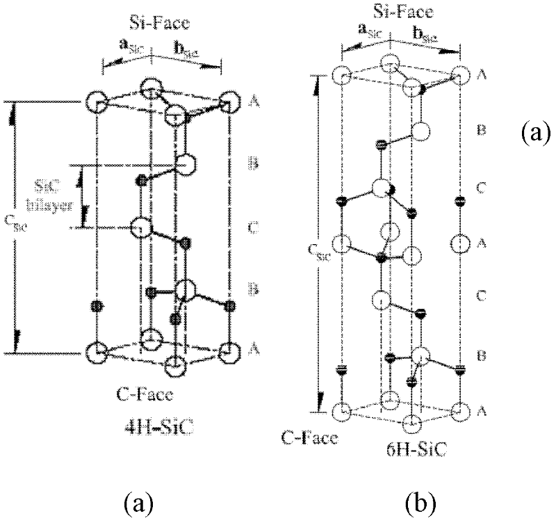
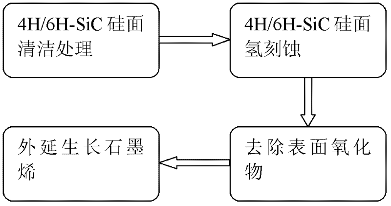
[0020] Embodiment 1, the steps of the present invention to epitaxially grow Graphene on the 4H-SiC(0001) silicon surface are as follows:

[0021] Step 1, remove sample surface pollutants.

[0022] Clean the silicon surface of 4H-SiC(0001). Place the SiC in deionized water for ultrasonic cleaning for 15 minutes, take it out, and rinse repeatedly; soak the SiC in a solution of ammonia: hydrogen peroxide: deionized water = 1:2:5, boil, soak for 15 minutes, and wash repeatedly with deionized water; SiC was immersed in hydrochloric acid: hydrogen peroxide: deionized water = 1:2:8 solution and boiled for 15min, then washed repeatedly with deionized water; put SiC in 5% HF solution for 1min, and rinsed with deionized water; place SiC in deionized water Clean in the ultrasonic wave of ion water for 15min, rinse repeatedly, take out and dry.

[0023] Step 2, performing hydrogen etching on the 4H-SiC(0001) silicon surface.

[0024] Place the cleaned 4H-SiC silicon surface in the CVD ...

Embodiment 2

[0029] Embodiment 2, the step of the present invention epitaxially growing graphene on the 6H-SiC silicon surface is as follows:

[0030] Step 1, cleaning the surface of the 6H-SiC(0001) silicon surface to remove pollutants on the sample surface.

[0031] 1a) Place the SiC in deionized water for ultrasonic cleaning for 15 minutes, take it out, and rinse repeatedly;

[0032] 1b) Soak the SiC in a solution of ammonia water: hydrogen peroxide: deionized water = 1:2:5, boil, soak for 15 minutes, and wash repeatedly with deionized water;

[0033] 1c) Immerse the SiC in a solution of hydrochloric acid: hydrogen peroxide: ionized water = 1:2:8 and boil for 15 minutes, then wash it repeatedly with deionized water;

[0034] 1d) Put SiC in 5% HF solution for 1 min, and rinse with deionized water;

[0035] 1e) Place the SiC in deionized water for ultrasonic cleaning for 15 minutes, rinse repeatedly, take it out and dry it.

[0036] Step 2, performing hydrogen etching on the 6H-SiC (00...

Embodiment 3

[0042] Embodiment 3, the steps of the present invention to epitaxially grow Graphene on the 6H-SiC silicon surface are as follows:

[0043] Step A, cleaning the surface of the 6H-SiC(0001) silicon surface to remove pollutants on the surface of the sample.

[0044] Place the SiC in the ultrasonic wave of deionized water and clean it for 15 minutes, take it out, and rinse it repeatedly;

[0045] Soak SiC in a solution of ammonia: hydrogen peroxide: deionized water = 1:2:5, boil, soak for 15 minutes, and wash repeatedly with deionized water;

[0046] Immerse SiC in a solution of hydrochloric acid: hydrogen peroxide: deionized water = 1:2:8, boil for 15 minutes, and wash with deionized water repeatedly;

[0047] Put SiC in 5% HF solution for 1min, rinse with deionized water;

[0048] Place the SiC in deionized water for ultrasonic cleaning for 15 minutes, rinse repeatedly, take it out and dry it.

[0049] Step B, performing hydrogen etching on the 6H-SiC (0001) silicon surface....


PUM

PropertyMeasurementUnit
densityaaaaaaaaaa

Abstract

The invention discloses a method for epitaxial growth of wafer-level graphene on a 4H / 6H-SiC (0001) surface. The method mainly solves the problem that based on the prior art, during epitaxial growth of graphene on a 4H / 6H-SiC surface, a graphene area is small and graphene uniformity is low. The method comprises the following steps of 1, cleaning a 4H / 6H-SiC (0001) surface to remove organic residues and ionic pollutants on the 4H / 6H-SiC (0001) surface, 2, feeding hydrogen, and carrying out hydrogen etching of the cleaned 4H / 6H-SiC (0001) surface to remove surface scratches so that regular bench-shaped stripes are formed, 3, feeding silane to remove oxides which are formed on the 4H / 6H-SiC (0001) surface by the hydrogen etching, and 4, heating in a low-argon pressure environment to evaporate silicon atoms so that carbon atoms are rearranged on the 4H / 6H-SiC (0001) surface by a sp2 method to form epitaxial graphene. Graphene obtained by the method has a large area and good uniformity and can be utilized for preparation of a wafer-level epitaxial graphene material.

Description

technical field [0001] The invention belongs to the technical field of microelectronics and relates to the manufacture of semiconductor materials, in particular to a method for preparing wafer-level graphene epitaxially grown on a 4H / 6H-SiC (0001) silicon surface. Background technique [0002] Graphene is composed of single layer sp 2 The material with hexagonal planar lattice structure composed of carbon atoms has excellent physical properties, mainly in the following aspects: (1) Strong bipolar electric field effect: only an external electric field is applied, and its charge carrier density is It can continuously change from n-type to p-type; (2) Near the Dirac point, electrons and holes show a linear dispersion relationship like photons. At low temperatures, the speed of electrons and holes is close to three times the speed of light in vacuum (3) At room temperature, the mobility of graphene electrons and holes reaches 2×10 4 cm 2 / V·s, whose value is 10 times higher t...

Claims


Application Information

Patent Timeline
Patent Type & Authority Applications(China)
IPC IPC(8): C30B25/02C30B25/18C30B29/20C23C16/26C23C16/02
Inventor 张玉明王党朝王悦湖雷天民张义门汤晓燕王航雷军
Owner XIDIAN UNIV
Why Eureka
Try Eureka