Metal grating coupling SPR (Surface Plasmon Resonance) detection chip and manufacturing method thereof

A metal grating and detection chip technology, which is applied in the measurement of color/spectral characteristics, etc., can solve the problems of time-consuming, expensive projection exposure machines, unfavorable exposure of large-area graphics, etc., to reduce process time and cost, and to benefit The effect of industrial mass production

Inactive Publication Date: 2012-05-02
SUZHOU INST OF NANO TECH & NANO BIONICS CHINESE ACEDEMY OF SCI
View PDF5 Cites 6 Cited by
  • Summary
  • Abstract
  • Description
  • Claims
  • Application Information

AI Technical Summary

Problems solved by technology

The electron beam exposure machine is mainly used for nanoscale pattern lithography. However, it performs read-write exposure on images one by one, which is not conducive to the exposure of large-area graphics and will take a lot of time; the stepper exposure machine can expose large-area images. However, the expensive projection exposure machine and the high-cost mask preparation process make the cost of lithography very high

Method used


Image

  • Metal grating coupling SPR (Surface Plasmon Resonance) detection chip and manufacturing method thereof
  • Metal grating coupling SPR (Surface Plasmon Resonance) detection chip and manufacturing method thereof
  • Metal grating coupling SPR (Surface Plasmon Resonance) detection chip and manufacturing method thereof

Examples


Embodiment 1

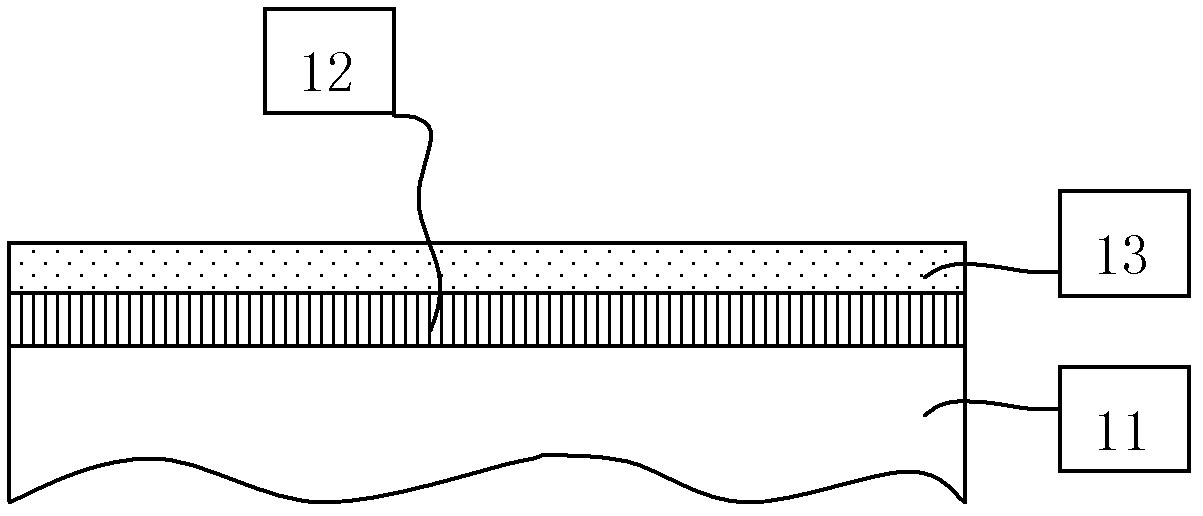
[0031] Example 1 refer to figure 1 , the metal grating coupling SPR detection chip includes: a transparent substrate 11, a metal grating coupling layer 12 and a microfluidic layer 13, the microfluidic layer is distributed with microfluidic channels bonded with the metal grating coupling layer; the microfluidic channel is bonded to the metal grating coupling layer; The grating coupling layer is cross-contacted.

[0032] The aforementioned transparent substrate is composed of a transparent organic material or a transparent inorganic material, preferably glass.

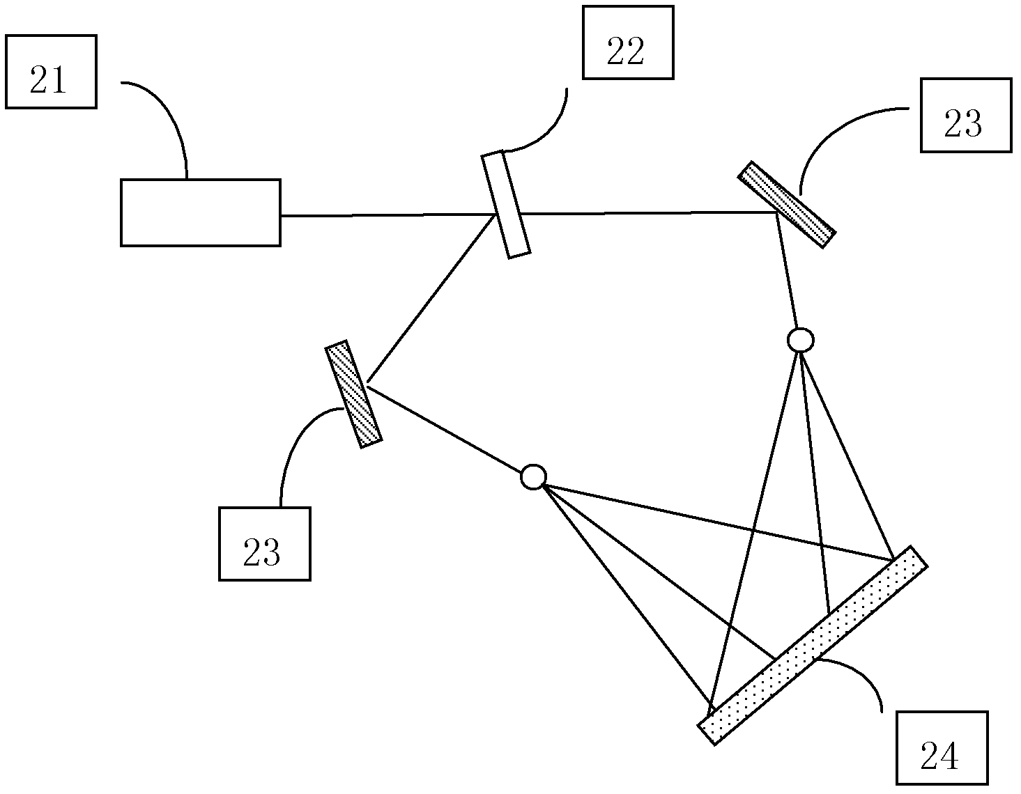
[0033] The aforementioned metal grating is prepared by laser holographic lithography process, and its principle can be found in figure 2 . A laser holographic lithography process is used to form a stripe grating on a photoresist layer evenly coated on the substrate surface. A metal film is formed on the above-mentioned stripe grating by using an electron beam evaporation process, and then the photoresist is strippe...


PUM

PropertyMeasurementUnit
thicknessaaaaaaaaaa

Abstract

The invention discloses a metal grating coupling SPR (Surface Plasmon Resonance) detection chip and a manufacturing method thereof. The detection chip comprises a transparent substrate, a metal grating coupling layer formed on the substrate, and a microfluid layer covered on the metal grating coupling layer. The manufacturing method comprises the following steps: applying a laser hologram photoetching process to form strip gratings on photoresist uniformly coated on the surface of the substrate, forming a metal film by a metal film coating process, further stripping the photoresist to obtain a metal grating coupling layer, and bonding the prepared microfluid layer and the metal grating coupling layer to obtain a target product. According to the invention, the laser hologram photoetching process is applied in the SPR detection chip, and in a grating manufacturing process, rapid and large-area exposure is available to obtain periodic striped patterns, i.e. one-dimensional gratings, so the process time and cost are greatly reduced, which is conductive to industrialized mass production.

Description

technical field [0001] The invention relates to a detection chip and a preparation method thereof in the technical field of surface plasmon resonance (SPR) biological and chemical detection, in particular to a metal grating coupling SPR detection chip based on a laser holographic photolithography process. Background technique [0002] Surface Plasmon Resonance (SPR) is an optical physical phenomenon. When incident light interacts with free electrons on the surface of the metal film, surface plasmon waves will be generated at the interface of the metal film. When the propagation constant of the incident light wave matches that of the surface plasmon wave, free electrons in the metal film are caused to resonate, that is, surface plasmon resonance. During the analysis, a layer of biomolecular recognition film is first fixed on the surface of the detection chip, and then the sample to be tested flows over the surface of the chip. If there are molecules in the sample that can in...

Claims


Application Information

Patent Timeline
Patent Type & Authority Applications(China)
IPC IPC(8): G01N21/25
Inventor 王逸群刘帆
Owner SUZHOU INST OF NANO TECH & NANO BIONICS CHINESE ACEDEMY OF SCI
Why Eureka
Try Eureka