Semiconductor PiP (package in package) system structure and manufacturing method thereof

A technology of packaging and system structure in packaging, which is applied in semiconductor/solid-state device manufacturing, semiconductor devices, semiconductor/solid-state device components, etc. The effect of wire bonding quality, preventing bridging phenomenon, and improving cutting efficiency

Inactive Publication Date: 2012-05-09
BEIJING UNIV OF TECH
View PDF4 Cites 14 Cited by
  • Summary
  • Abstract
  • Description
  • Claims
  • Application Information

AI Technical Summary

Problems solved by technology

[0004] With the improvement of IC integration and the continuous enhancement of functions, the number of I / Os of ICs increases, and the number of I / O pins of corresponding electronic packages also increases accordingly, and gradually changes from traditional two-dimensional planar packaging to more The development of highly integrated three-dimensional three-dimensional packaging forms, the traditional quadrilateral flat no-lead package is a typical two-dimensional planar packaging form, and the pins of a single circle are arranged around the chip carrier in a peripheral arrangement, which limits the increase in the number of I / Os and meets Does not meet the needs of high-density ICs with more I / O counts
The traditional lead frame has no step structure design, which cannot effectively lock the plastic material, resulting in low bonding strength between the lead frame and the plastic packaging material, which is easy to cause delamination of the lead frame and the plastic packaging material or even the falling off of the pin or chip carrier, and cannot effectively Prevent moisture from diffusing into the electronic package along the interface between the lead frame and the plastic packaging material, which seriously affects the reliability of the package
Traditional QFN products need to paste tape on the back of the lead frame in advance to prevent overflow during the plastic packaging process. After plastic packaging, cleaning processes such as removing the tape and molding compound flash need to be performed, which increases the packaging cost.
Use a dicing knife to cut and separate traditional quad flat no-lead packages. The dicing knife will also cut the lead frame metal while cutting the plastic packaging material, which will not only reduce the cutting efficiency and shorten the life of the dicing blade, but also produce metal burrs. , affecting the reliability of the package

Method used


Image

  • Semiconductor PiP (package in package) system structure and manufacturing method thereof
  • Semiconductor PiP (package in package) system structure and manufacturing method thereof
  • Semiconductor PiP (package in package) system structure and manufacturing method thereof

Examples


Embodiment Construction

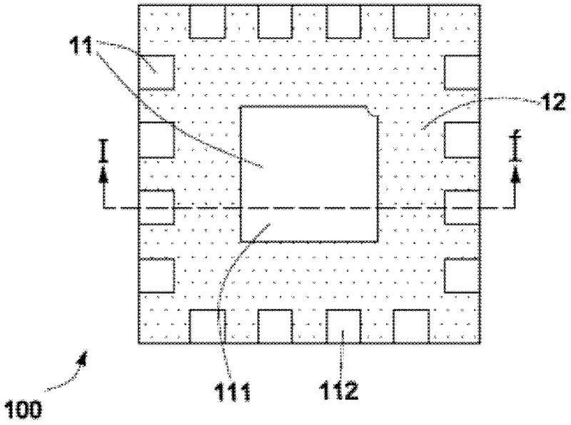
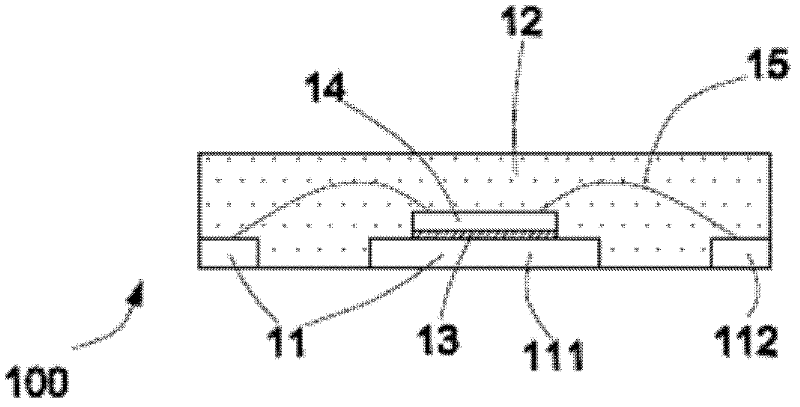
[0066] The present invention is described in detail below in conjunction with accompanying drawing:

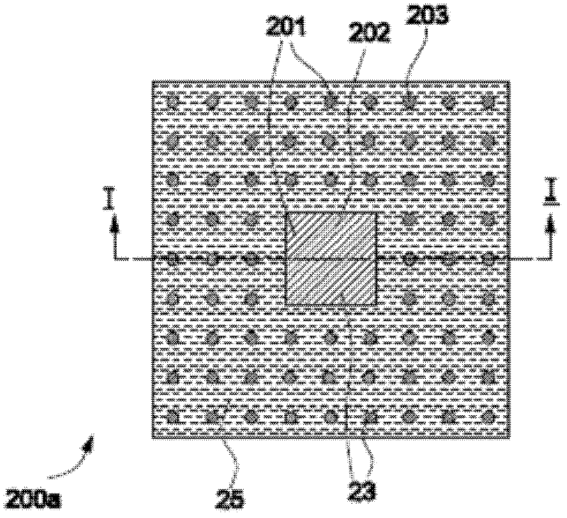
[0067] Figure 2A A schematic diagram of the rear side of a semiconductor package-in-package (PiP) system structure in which the cross-section of the pins is circular and the pins on each side of the chip carrier are arranged in parallel according to the embodiment of the present invention. Figure 2B A schematic diagram of the rear side of a semiconductor package-in-package (PiP) system structure drawn for an embodiment of the present invention in which the cross-section of the pins is rectangular and the pins on each side of the chip carrier are arranged in parallel.

[0068] Refer to the above Figure 2A -B It can be seen that, in this embodiment, the lead frames 201 of the semiconductor package-in-package (PiP) system structures 200a and 200b include a chip carrier 202 and pins 203 arranged in multiple circles around the chip carrier 202, and the chip carrier 202 The pin...


PUM


Abstract

The invention discloses a semiconductor PiP (package in package) system structure and a manufacturing method thereof. The semiconductor PiP system structure comprises a lead frame, a first metal material layer, a second metal material layer, an IC (integrated circuit) chip provided with salient points, a lead bonding IC chip, an insulating filling material, a pasting material and a plastic package material, wherein the lead frame comprises a chip carrier and multiple pins which surround the chip carrier and are arranged in multiple circles; the first metal material layer and the second metal material layer are respectively positioned on the upper surface and lower surface of the lead frame, and the insulating filling material is positioned below a terraced structure of the lead frame; the lead bonding IC chip is positioned on the chip carrier; and the salient points of the IC chip provided with the salient points are positioned on the inner pins of multiple circles of the pins in a flip-chip bonding manner, the plastic package material is used for coating the IC chip provided with the salient points and the lead bonding IC chip, thus forming the semiconductor PiP system structure. The invention relates to a three-dimensional package structure which has the advantages of high reliability, low cost and high I/O (input/output) density and is based on QFN (quad flat no-lead) package and a manufacturing method thereof.

Description

technical field [0001] The invention relates to the technical field of manufacturing semiconductor components, in particular to a QFN package-based semiconductor package in package (Package in Package, PiP) system structure, and the invention also includes a manufacturing method of the package. Background technique [0002] With the development of electronic products such as mobile phones and notebook computers towards miniaturization, portability, ultra-thinness, multimedia and low-cost requirements for popularization, high-density, high-performance, high-reliability and low-cost packaging forms and Its assembly technology has been developed rapidly. Compared with the expensive BGA and other packaging forms, the new packaging technology developed rapidly in recent years, that is, the quad flat non-lead QFN (Quad Flat Non-lead Package) package, due to its good thermal performance and electrical performance, small size, Many advantages such as low cost and high productivity ...

Claims


Application Information

Patent Timeline
Patent Type & Authority Applications(China)
IPC IPC(8): H01L23/488H01L23/495H01L23/31H01L21/50H01L21/60H01L21/56H01L21/78
CPCH01L23/49861H01L23/3121H01L2224/73265H01L21/4828H01L21/78H01L21/561H01L2224/16245H01L2224/48091H01L2224/97H01L25/03H01L23/488H01L2924/30107H01L24/16H01L24/48H01L2924/3011H01L2224/32245H01L21/56H01L2224/48247H01L2224/92247H01L2224/48095H01L23/31H01L24/97H01L24/32H01L23/49575H01L2224/48227H01L2924/00014H01L2924/181H01L23/49544H01L24/73H01L2224/45144H01L2224/45147H01L2924/14H01L2224/45124H01L2224/45565H01L2224/45664H01L2224/29339H01L2224/2929H01L24/45H01L2224/83101H01L2224/45099H01L2924/00012H01L2924/00H01L2924/0665H01L2224/05599H01L24/85H01L24/81H01L21/4821H01L2924/171H01L23/142H01L23/52H01L23/28
Inventor 秦飞夏国峰安彤刘程艳武伟朱文辉
Owner BEIJING UNIV OF TECH
Why Eureka
Try Eureka