Array base plate, liquid crystal display and manufacturing method for array base plate
A manufacturing method and array substrate technology, which is applied in semiconductor/solid-state device manufacturing, instruments, electric solid-state devices, etc., can solve problems such as damage to TFT channels, achieve the effects of improving performance, reducing the number of photolithography times, and improving production efficiency
- Summary
- Abstract
- Description
- Claims
- Application Information
AI Technical Summary
Problems solved by technology
Method used
Image

Examples
Embodiment 1
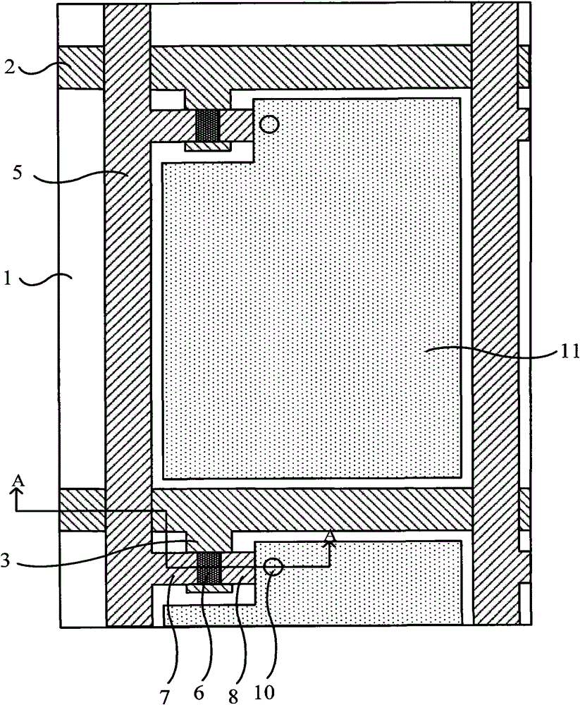
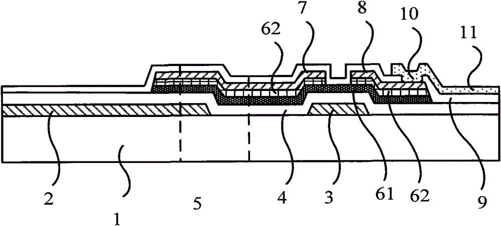
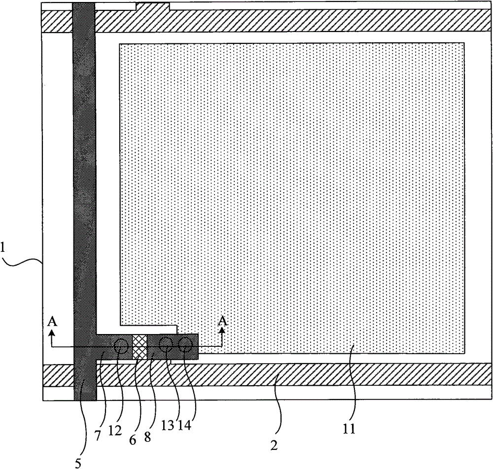
[0060] Figure 2A A partial top view structural schematic diagram of the array substrate provided by Embodiment 1 of the present invention; Figure 2B for Figure 2A Schematic diagram of the cut-away structure in side view along line A-A. Such as Figure 2A and Figure 2B As shown, the array substrate of this embodiment includes: a base substrate 1 on which gate lines 2, data lines 5, thin film transistors (TFT), pixel electrodes 11, active layer 6, and passivation layer 9 are formed. and gate insulating layer 4. Wherein, the TFT includes a gate electrode 3 , a source electrode 7 and a drain electrode 8 ; the gate electrode 3 is connected to the gate line 2 , the source electrode 7 is connected to the data line 5 , and the drain electrode 8 is connected to the pixel electrode 11 . Wherein, the gate insulating layer 4 is formed above the gate electrode 3; the active layer 6 is formed above the gate insulating layer 4; the passivation layer 9 is formed above the active laye...
Embodiment 2
[0085] Figure 6A It is a flow chart of the manufacturing method of the array substrate provided by Embodiment 2 of the present invention. Such as Figure 6A As shown, the method of the present embodiment includes:
[0086] Step 61, depositing a transparent conductive film and a gate metal film on the base substrate, and forming a pattern including a pixel electrode, a gate electrode and a gate line through a patterning process;
[0087] Step 62, depositing a gate insulating layer film, an active layer film and a passivation layer film on the base substrate forming the above pattern, and forming a pattern including a passivation layer, an active layer and a gate insulating layer through a patterning process; wherein, the passivation layer The gate insulating layer includes a source electrode via hole and a drain electrode via hole; the gate insulating layer includes a contact via hole, and the contact via hole is located above the pixel electrode;
[0088] Step 63. Deposit ...
PUM
 Abstract
Description
Claims
Application Information
 - R&D
- Intellectual Property
- Life Sciences
- Materials
- Tech Scout
- Unparalleled Data Quality
- Higher Quality Content
- 60% Fewer Hallucinations
Browse by: Latest US Patents, China's latest patents, Technical Efficacy Thesaurus, Application Domain, Technology Topic, Popular Technical Reports.
© 2025 PatSnap. All rights reserved.Legal|Privacy policy|Modern Slavery Act Transparency Statement|Sitemap|About US| Contact US: help@patsnap.com