Semiconductor chip assembly with post/base heat spreader and cavity over post

A technology for semiconductors and chipsets, applied in semiconductor devices, semiconductor/solid-state device components, and electrical solid-state devices, etc., and can solve problems such as excessive volume, reduced heat dissipation, and limited routing capabilities.

Inactive Publication Date: 2012-05-16
BRIDGE SEMICON
View PDF15 Cites 17 Cited by
  • Summary
  • Abstract
  • Description
  • Claims
  • Application Information

AI Technical Summary

Problems solved by technology

If the substrate is a single-layer circuit system, the routing capability is limited, but if the substrate is a multi-layer circuit system, its excessively thick dielectric layer will reduce the heat dissipation effect
In addition, the previous technol...

Method used


Image

  • Semiconductor chip assembly with post/base heat spreader and cavity over post
  • Semiconductor chip assembly with post/base heat spreader and cavity over post
  • Semiconductor chip assembly with post/base heat spreader and cavity over post

Examples


Embodiment Construction

[0119] The present invention will be described in detail below in conjunction with the accompanying drawings and embodiments. The embodiments described herein are for illustration purposes, and the related elements or steps of the present technology are simplified or omitted to avoid obscuring the characteristics of the present invention. Likewise, elements and reference numerals that are repeated or not necessary in the drawings may be omitted for clarity of the drawings.

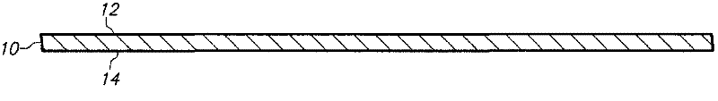
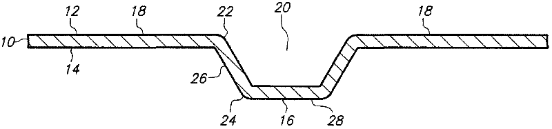
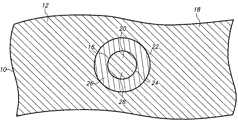
[0120] figure 1 and figure 2 It is a cross-sectional view illustrating a method of manufacturing a bump and an outrigger platform in an embodiment of the present invention, image 3 and Figure 4 respectively figure 2 top and bottom views.

[0121] figure 1 Is a cross-sectional view of a metal plate 10 comprising opposing major surfaces 12 and 14 . The illustrated metal plate 10 is a copper plate having a thickness of 70 microns. Copper has the advantages of high thermal conductivity, good bondin...


PUM


Abstract

The invention relates to a semiconductor chip assembly with a post/base heat spreader and a cavity over post. The semiconductor chip assembly at least includes a semiconductor device, the heat spreader, the substrate and an adhesive. The semiconductor device is electrically connected to the substrate and thermally connected to the heat spreader. The heat spreader at least includes a post and a base. The post extends upwardly from the base into an opening in the adhesive and an aperture in the substrate, and the base extends laterally from the post. The adhesive extends between the post and the substrate and between the base and the substrate. The assembly provides signal routing between a pad and a terminal.

Description

technical field [0001] The invention relates to a semiconductor chip assembly body, more specifically, a semiconductor chip assembly body with semiconductor elements, wires, adhesive layers and heat sinks and a manufacturing method thereof. Background technique [0002] Existing semiconductor components such as packaged and unpackaged semiconductor chips can provide high-voltage, high-frequency and high-performance applications; these applications require high power consumption to perform specific functions, but the higher the power, the semiconductor Components generate more heat. In addition, after the packaging density is increased and the size is reduced, the surface area available for heat dissipation is reduced, which leads to serious accumulation of heat energy. [0003] Semiconductor components are prone to problems such as performance degradation and shortened service life under high temperature operation, and may even fail immediately. High heat not only affects ...

Claims


Application Information

Patent Timeline
IPC IPC(8): H01L23/367H01L23/31H01L33/64H01L33/48
CPCH01L2224/32245H01L2224/48091H01L2224/73265H01L2224/48247H01L2924/12041H01L2224/48227H01L2924/3025H01L24/73H01L2924/00012H01L2924/00014H01L2924/00
Inventor 林文强王家忠
Owner BRIDGE SEMICON
Why Eureka
Try Eureka