Heating device for semiconducting material hot wall epitaxy growth system

A hot-wall epitaxy and heating device technology, which is applied in the directions of polycrystalline material growth, crystal growth, single crystal growth, etc., can solve the problems that the heating method cannot meet the use requirements, the ultra-large diameter reaction chamber is not suitable, and the heating and cooling speed is slow. , to achieve the effect of mass production, long service life, and rapid heating and cooling

Active Publication Date: 2012-05-23
NANJING UNIV
View PDF7 Cites 3 Cited by
  • Summary
  • Abstract
  • Description
  • Claims
  • Application Information

AI Technical Summary

Problems solved by technology

[0005] The technical problem to be solved by the present invention is: the heating method of the existing hot-wall epitaxial growth system cannot meet t

Method used


Image

  • Heating device for semiconducting material hot wall epitaxy growth system
  • Heating device for semiconducting material hot wall epitaxy growth system

Examples


Embodiment Construction

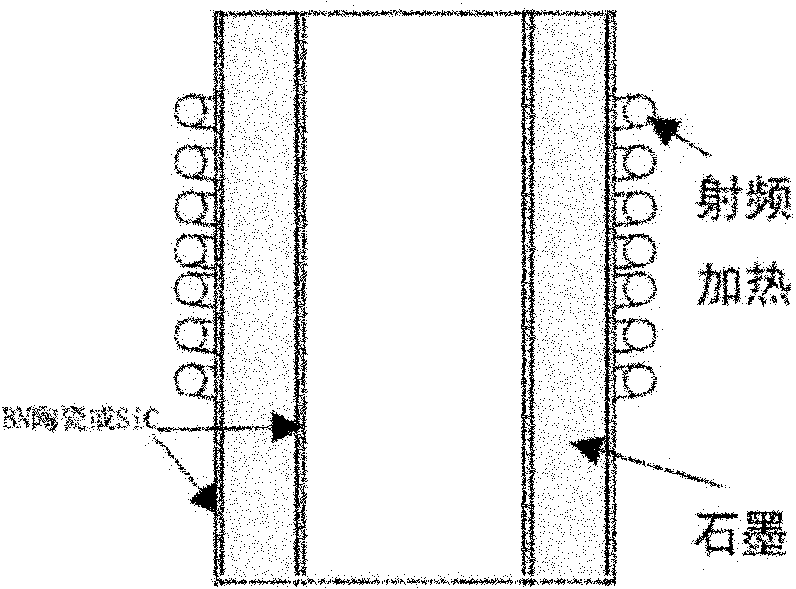
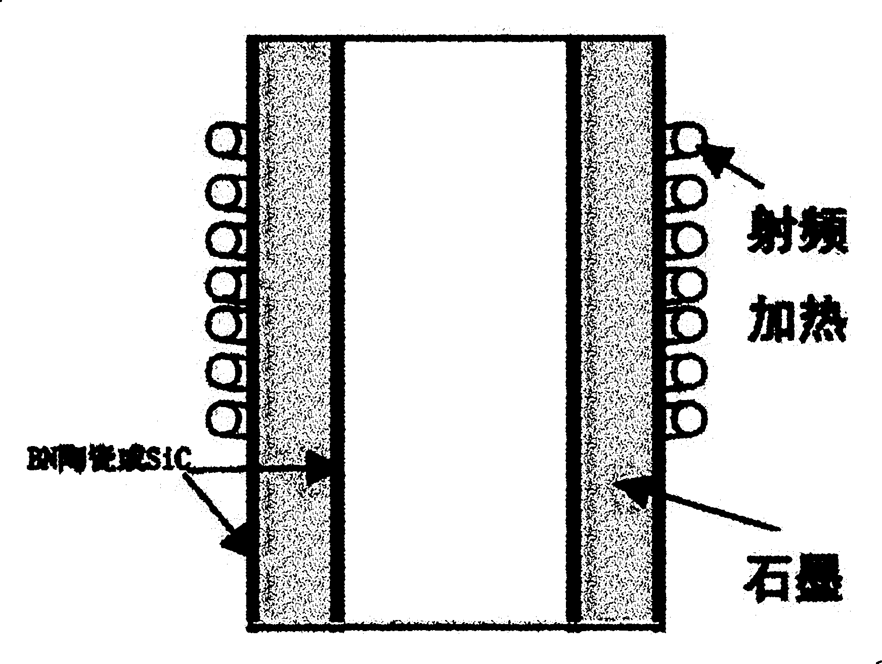
[0014] The present invention adopts radio frequency heating method, such as figure 1 As shown, the graphite sleeve is set in the induction heating coil of the radio frequency heater, and the graphite sleeve is heated by radio frequency to form a hot wall environment. The reaction chamber of the semiconductor growth system is set in the graphite sleeve, and the reaction chamber is a graphite support. The grown semiconductor material sample is placed on a graphite support. The principle of radio frequency heating is: the inductor of the radio frequency heater is generally a hollow copper tube that inputs intermediate frequency or high frequency alternating current (1000-300000Hz or higher). Put the conductive graphite sleeve into the induction heating coil, and use the principle of electromagnetic induction heating to generate an alternating magnetic field to generate an induced current of the same frequency in the graphite, heat the graphite sleeve, and convert electrical energ...


PUM


Abstract

The invention relates to a heating device for a semiconducting material hot wall epitaxy growth system, which comprises a radio-frequency heater and a graphite sleeve, wherein the graphite sleeve is arranged in an induction heating coil of the radio-frequency heater; the inner wall and the outer wall of the graphite sleeve are respectively coated with a heat-conduction and noncombustible insulating layer; and the graphite sleeve is placed in an inert gas environment. The heating device provided by the invention adopts radio-frequency for heating the graphite sleeve, can be used for quickly heating and cooling, and has the advantages of energy conservation, long service life, maintenance-free and the like. Since the diameter of the induction heating coil can be enlarged, quick heating of a large-area reaction chamber can be realized through heating the large-sized graphite sleeve.

Description

technical field [0001] The invention relates to a semiconductor material growth system, in particular to a heating device for a semiconductor material hot wall epitaxial growth system. Background technique [0002] Group III-V nitride materials (also known as GaN-based materials) mainly composed of GaN, InGaN, and AlGaN alloy materials are new semiconductor materials that have attracted much attention in the world in recent years. GaN-based materials are direct bandgap wide-bandgap semiconductor materials with continuously variable direct bandgap between 1.9-6.2eV, excellent physical and chemical stability, high saturation electron drift velocity, high breakdown field strength and high thermal conductivity It has important applications in the preparation of short-wavelength semiconductor optoelectronic devices and high-frequency, high-voltage, and high-temperature microelectronic devices. It is used to manufacture light-emitting devices and detectors such as blue, purple, an...

Claims


Application Information

Patent Timeline
IPC IPC(8): C30B25/10C30B29/40
Inventor 修向前张荣谢自力华雪梅韩平陆海顾书林施毅胡立群郑有炓
Owner NANJING UNIV
Why Eureka
Try Eureka