Semiconductor laser source

A laser light source and semiconductor technology, applied in the direction of semiconductor lasers, semiconductor laser devices, lasers, etc., can solve the problems of large volume, complex structure, and high requirements for operators, and achieve strong flexibility, convenient adjustment, and ensure efficiency and stability. Effect

Inactive Publication Date: 2012-05-23
PHOEBUS VISION OPTO ELECTRONICS TECH
View PDF3 Cites 0 Cited by
  • Summary
  • Abstract
  • Description
  • Claims
  • Application Information

AI Technical Summary

Problems solved by technology

[0005] In order to solve the problems of large volume, complex structure and high requirements for operators in the prior art, the present invention provides a semiconductor laser light source with small volume, simple structure and easy operation

Method used


Image

  • Semiconductor laser source
  • Semiconductor laser source
  • Semiconductor laser source

Examples


Embodiment 1

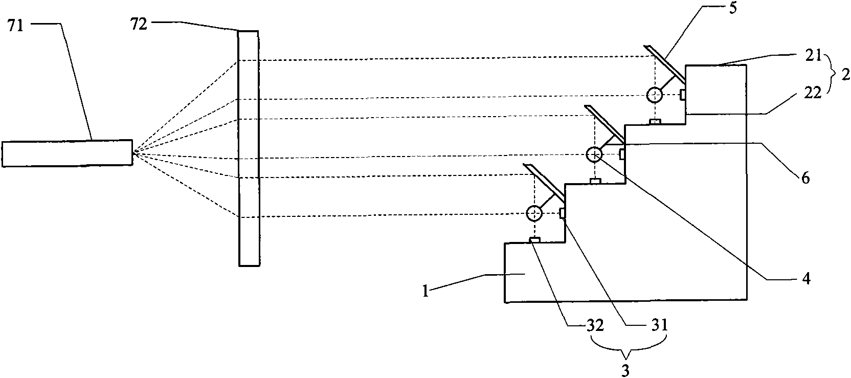
[0027] figure 1 It is a schematic diagram of the working principle of a specific embodiment of the semiconductor laser light source of the present invention.

[0028] A heat sink with N steps, each of which includes a vertical mounting surface and a horizontal mounting surface, wherein N is a natural number; 2 (N-1) semiconductor lasers, including (N -1) first semiconductor lasers and (N-1) second semiconductor lasers arranged on the horizontal mounting surface, the optical axis of the output light of the first semiconductor laser is perpendicular to the vertical mounting surface, and the output light of the second semiconductor laser The optical axis is perpendicular to the horizontal installation surface, and the first semiconductor laser intersects at a point the output light optical axis of the second semiconductor laser arranged on the horizontal installation surface of the next step; it is arranged above each second semiconductor laser for adjustment The reflector of th...

Embodiment 2

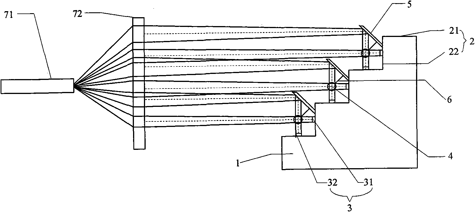
[0047] figure 2 It is a schematic diagram of the working principle of another specific embodiment of the semiconductor laser light source of the present invention.

[0048] see figure 2 As shown, the semiconductor laser light source disclosed in the present invention has the same main structure as that of Embodiment 1, the difference is that the output light of the semiconductor laser 3 is not exactly the same wavelength of light, and the divergence angles of the output light of each semiconductor laser 3 are different. , overlap is allowed between the collimated beams.

[0049] Therefore, in this embodiment, the red, blue, and green semiconductor lasers can be arranged on a stepped heat sink to be used as a white light source.

Embodiment 3

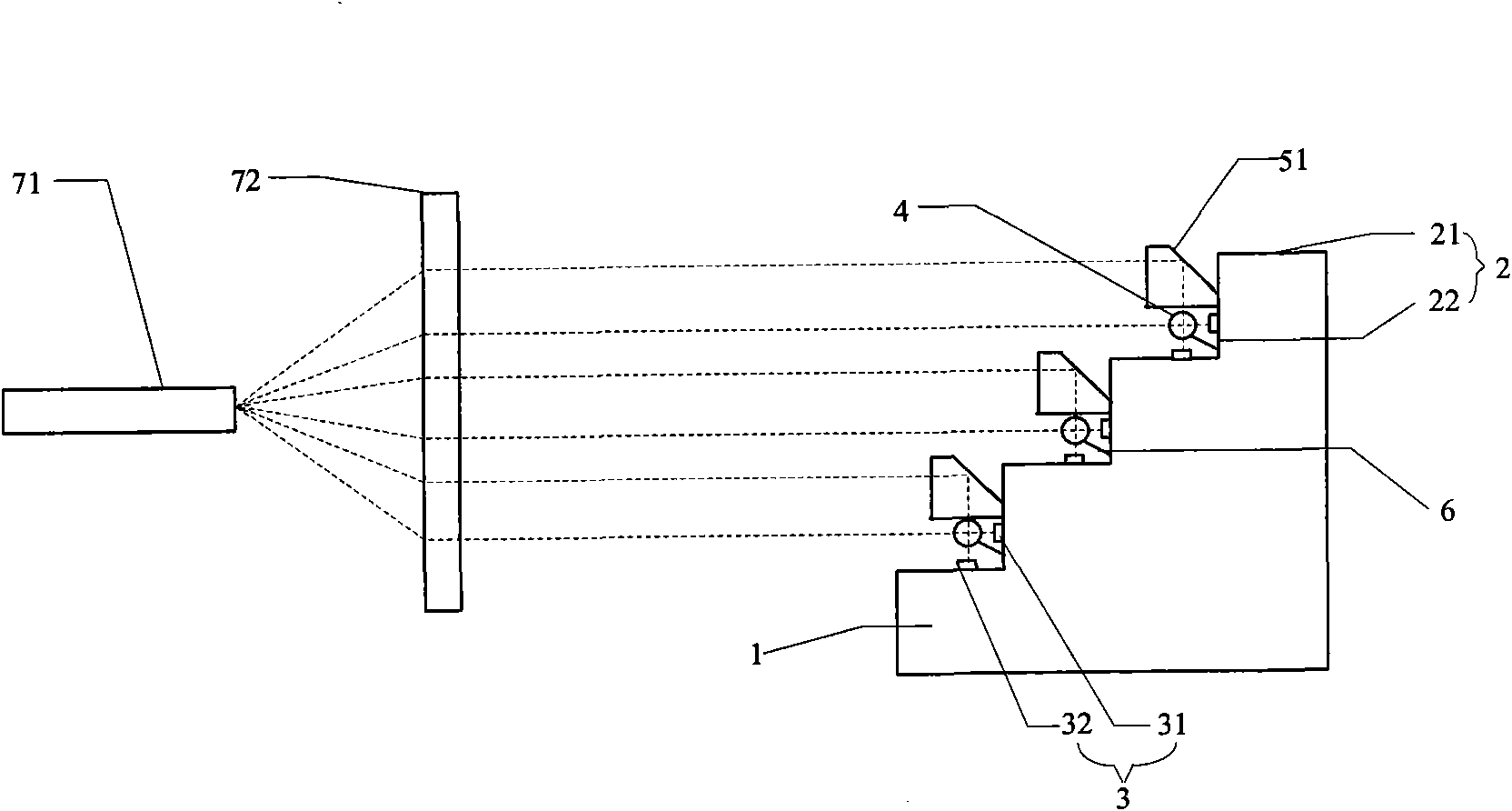
[0051] image 3 It is a schematic diagram of the working principle of another specific embodiment of the semiconductor laser light source of the present invention.

[0052] see image 3 As shown, the semiconductor laser light source disclosed in the present invention has a heat sink 1 with four steps 2, and each step 2 includes a vertical installation surface 22 and a horizontal installation surface 21;

[0053] 6 semiconductor lasers, including 3 first semiconductor lasers 31 arranged on the vertical mounting surface 22 and 3 second semiconductor lasers 32 arranged on the horizontal mounting surface 21, the uppermost one horizontal mounting surface 21 and the lowermost one No semiconductor laser is arranged on the vertical mounting surface 22, the output light optical axis of the first semiconductor laser 31 is perpendicular to the vertical mounting surface 22, the output light optical axis of the second semiconductor laser 32 is perpendicular to the horizontal mounting surf...


PUM


Abstract

The invention discloses a semiconductor laser source, comprising a heat sink with N steps, 2N semiconductor lasers, reflectors and N micro lenses, wherein each step comprises a vertical installation face and a horizontal installation face; N is a natural number; the 2N semiconductor lasers comprise (N-1) first semiconductor lasers which are arranged on the vertical installation face and (N-1) second semiconductor lasers which are arranged on the horizontal installation face; the optical axes of output light of the first semiconductor lasers and the second semiconductor lasers arranged on the steps below the first semiconductor lasers are crossed at a point; the reflectors are arranged above the second semiconductor lasers for adjusting the direction of the optical axes of the output light of the second semiconductor lasers; and the N micro lenses are used for aligning the output light of the semiconductor lasers so that an aligned light beam which is aligned by a corresponding micro lens array is formed by the output light of the semiconductor lasers. The semiconductor laser source provided by the invention has the advantages of simple structure and convenience for adjustment, and can ensure the efficiency and the stability of laser coupling. Therefore, the semiconductor laser source is applicable to modularization production in a large scale.

Description

technical field [0001] The invention relates to a semiconductor laser light source, in particular to the optical fiber coupling technology of the semiconductor laser. Background technique [0002] Semiconductor laser is the most important type of laser in practical use. It has the advantages of small size, long life, reliable operation, and low power consumption. It is used in laser communication, optical storage, optical gyroscope, laser printing, ranging, and radar. Widely, semiconductor lasers (LDs) are often used as light sources in laser displays or other occasions that require high-brightness and high-beam quality lasers, because semiconductor lasers have the problem that the output light is a divergent beam and the power density is relatively low. Lasers often cannot meet the requirements of laser displays for light sources. In practical applications, it is often necessary to couple the output light of multiple semiconductor lasers before outputting. At present, the...

Claims


Application Information

Patent Timeline
Patent Type & Authority Applications(China)
IPC IPC(8): H01S5/40H01S5/024H01S5/068
Inventor 桂周琦毕勇张瑛房涛
Owner PHOEBUS VISION OPTO ELECTRONICS TECH
Why Eureka
Try Eureka