Ceramic substrate for mounting luminescent element

A ceramic substrate and light-emitting element technology, which is applied in electrical components, ceramic products, applications, etc., can solve the problems of reduced reflectivity, substrate shedding, etc., and achieve the effect of improving reflectivity

Inactive Publication Date: 2012-05-23
KYOCERA CORP
View PDF8 Cites 6 Cited by
  • Summary
  • Abstract
  • Description
  • Claims
  • Application Information

AI Technical Summary

Problems solved by technology

In addition, for the type of coating the reflective material on the substrate, the reflectivity will decrease due to the color change of the reflective material over time, or the reflective material will fall off from the substrate due to the heat dissipation of the light-emitting element. high reflectivity

Method used


Image

  • Ceramic substrate for mounting luminescent element
  • Ceramic substrate for mounting luminescent element
  • Ceramic substrate for mounting luminescent element

Examples


Embodiment 1

[0060] Hereinafter, examples of the present invention will be specifically described, but the present invention is not limited to the following examples.

[0061] First, prepare as alumina (Al 2 o 3 ) powder with an average particle size of about 1.6 μm, silicon oxide (SiO 2 ), and at least one powder of calcium oxide (CaO) and magnesium oxide (MgO). Then, the mixed powder weighed so that the total content of each powder becomes 100% by mass is put into a tumbler together with a solvent such as water, and mixed.

[0062] Next, an acrylic resin molding binder was added thereto, and high-purity alumina balls were further mixed with a tumbler to obtain a slurry. Here, the added amount of the molding binder is set to about 4 to 8 mass % with respect to 100 mass % of the mixed powder. If it is within this range, there will be no problem with the strength and flexibility of the molded article, and there will be no problem of insufficient degreasing of the molding binder during f...

Embodiment 2

[0085] Next, the relationship with the reflectance due to the fact that the number of pores on the central portion side is larger than that on the front side of the ceramic substrate 1 for mounting a light emitting element is investigated.

[0086] First, using the same raw material as sample No. 12 produced in Example 1, a molded body was produced in the same process as in Example 1, and the rate of increase and decrease in the firing temperature and firing time shown in Table 3 Under the condition of firing, the substrate 1 is produced.

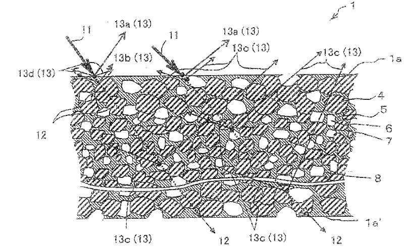
[0087]The measuring method of the porosity is the same as in Example 1. However, when measuring the number of pores on the central portion side, since the thickness of the base 1 is 0.635 mm, the base 1 is ground about 0.32 mm from the surface 1 a, and the polished surface is measured in the same manner as in Example 1. In addition, as for the reflectance, it measures here only at a wavelength of 500 nm.

[0088] Table 3 shows the obtaine...

Embodiment 3

[0093] The average pore diameter and wavelength Measurement of the reflectivity of 200-350nm.

[0094] Table 4 shows the obtained results.

[0095] Table 4

[0096]

[0097] From the results in Table 4, it can be seen that the reflectance of the sample No. 1 of the comparative example whose average pore diameter is as high as 2.02 μm has a wavelength of 350 nm or less decreases rapidly. In addition, when the average pore diameter is as small as 0.95 μm, the reflectance at a wavelength of 250 nm or less becomes low.

[0098] Sample Nos. 5, 12 and 13 of the examples of this embodiment have an average pore diameter in the range of 1.00 to 1.95 μm, reflectance to a wavelength of 300 nm is more than 80%, and a wavelength of 250 nm is more than 60%, which can significantly improve The reflectance in the ultraviolet region that becomes the problem.

[0099] Although the effect of the average pore diameter on this result is unknown, it is known that the average pore diameter is...


PUM

PropertyMeasurementUnit
pore sizeaaaaaaaaaa
thicknessaaaaaaaaaa
bending strengthaaaaaaaaaa

Abstract

Provided is a ceramic substrate for mounting a luminescent element thereon which has a reflectance as high as 90% or above in the ultraviolet to the infrared regions (350-1,000 nm) and which has satisfactory mechanical properties. The ceramic substrate (1) for mounting a luminescent element thereon comprises 94-97 mass% aluminum oxide and further contains silicon oxide and at least calcium oxide or magnesium oxide. In a surface (1a) of the substrate (1), when a portion having a surface area of 9.074105 [mu]m2 is examined with respect to pores having an equivalent-circle diameter of 0.8 [mu]m or larger, the porosity is 2.5-4.5%, the number of the pores is 7,000-11,000, and the cumulative relative frequency of pores having an equivalent-circle diameter of 1.6 [mu]m or smaller in the pore size distribution is 70% or higher. This substrate (1) has a reflectance as high as 90% or above in the ultraviolet to the infrared regions and satisfactory mechanical properties, and is suitable for use in a luminescent device (21).

Description

technical field [0001] The present invention relates to a ceramic substrate for mounting a light-emitting element for mounting a light-emitting element such as an LED. Background technique [0002] In recent years, LEDs (Light Emitting Diodes) have attracted attention as light-emitting elements with high luminance and low power consumption that can be mass-produced. Furthermore, they are widely used as light sources for general lighting or light sources for electro-optic display panels, and further, as backlights for image display devices using liquid crystals, such as mobile phones, computers, and televisions. [0003] Insulation required for forming electrodes on the surface of a substrate for mounting such a light-emitting element is pursued. In addition, for the type of coating the reflective material on the substrate, the reflectivity will decrease due to the color change of the reflective material over time, or the reflective material will fall off from the substrate ...

Claims


Application Information

Patent Timeline
Patent Type & Authority Applications(China)
IPC IPC(8): C04B38/00C04B35/111H01L33/48
CPCC04B2235/3418C04B2235/3206C04B38/0051H01L33/60C04B2235/775C04B2235/6567C04B2235/3208C04B2235/9646C04B2235/77C04B2235/96C04B35/111C04B2235/656C04B38/007C04B35/10H01L2224/48091H01L2224/73265H01L2224/45147H01L2924/01015H01L2924/01047H01L2924/181H01L2924/00011H01L2224/32225H01L2924/00014Y10T428/249969Y10T428/249921H01L2224/48227H01L2924/00H01L2924/00012H01L2224/45099H01L2924/01033H01L33/48
Inventor 内野和仁西本健一
Owner KYOCERA CORP
Why Eureka
Try Eureka