
Circuit used for programming resistance memory

A resistance memory and circuit technology, applied in the field of information storage, can solve the problems of increased circuit complexity, shrinkage, and low writing and erasing speed of floating gate memory, and achieve the effect of improving distribution uniformity and reliability

Active Publication Date: 2014-05-14
INST OF MICROELECTRONICS CHINESE ACAD OF SCI
View PDF3 Cites 0 Cited by
  • Summary
  • Abstract
  • Description
  • Claims
  • Application Information

AI Technical Summary

Problems solved by technology

[0003] However, with the technological upgrading and upgrading of the semiconductor industry, the shortcomings of floating gate memory are becoming more and more obvious.
First, the floating gate memory will encounter great difficulties in the process of shrinking the 60nm to 45nm process, because its charge writing and erasing mechanism requires the gate to be kept at a certain thickness, which cannot be compared with the device size. shrink together
Second, the floating gate memory cell uses channel hot electron injection to write charges to the floating gate, and the source-drain voltage must be greater than or equal to 3.2V to enable the channel electrons to obtain enough energy to pass through the tunneling dielectric layer. The power consumption of the floating gate memory is reduced
Third, the writing and erasing speed of floating gate memory is low, and the current product indicators are all on the order of microseconds, which greatly limits its application range, especially when integrated into embedded systems
This greatly increases the complexity of the circuit

Method used


Image

  • Circuit used for programming resistance memory
  • Circuit used for programming resistance memory
  • Circuit used for programming resistance memory

Examples


Embodiment Construction

[0027] In order to make the object, technical solution and advantages of the present invention clearer, the present invention will be described in further detail below in conjunction with specific embodiments and with reference to the accompanying drawings.

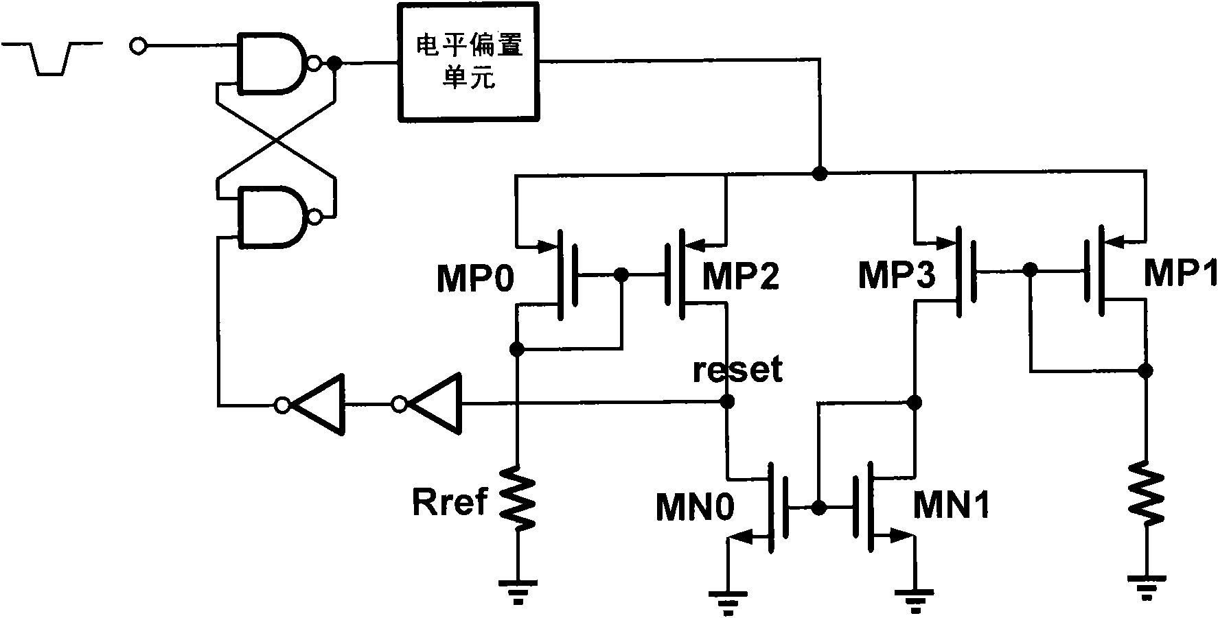
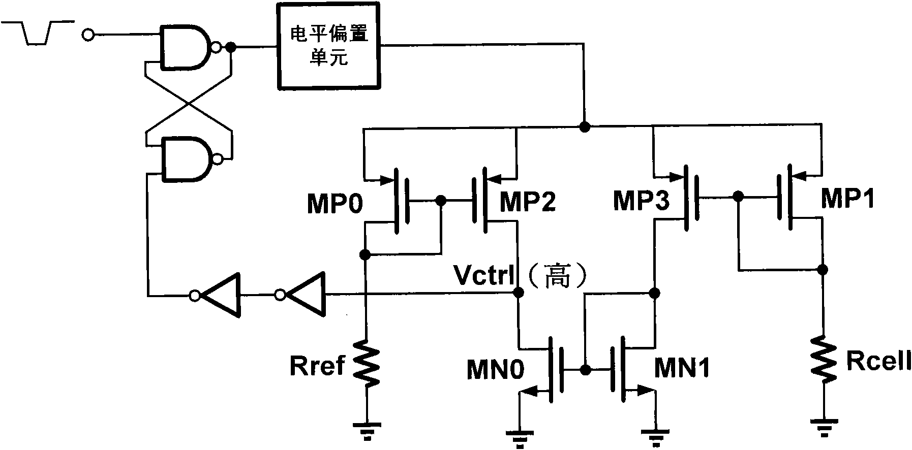
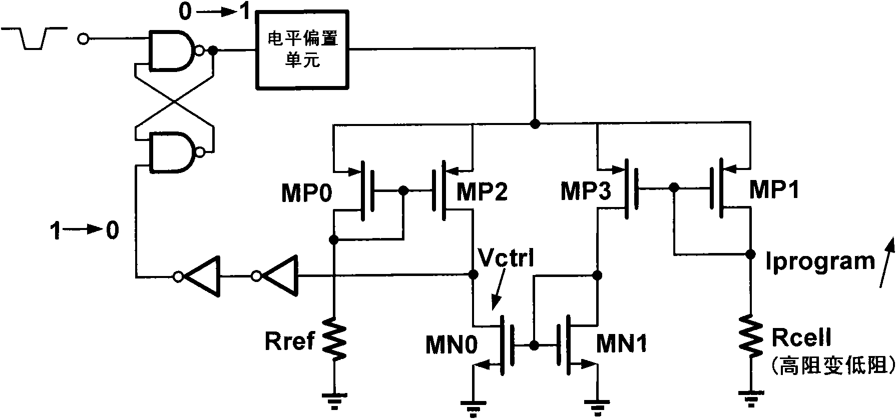
[0028] Taking the programming circuit that drives the resistance transition memory from high resistance to low resistance as an example, figure 1 is its schematic diagram. The circuit is composed of an RS flip-flop, a level bias unit, a current mirror, a current comparison circuit and an inverter. The output of the RS flip-flop controls the level bias unit; the level output by the level bias unit is used to program or erase the resistance memory; the signal returned by the feedback unit resets the RS flip-flop.

[0029] Among them, the RS flip-flop is composed of two double-input NAND gates, the input valid enabling level is low level, and the output valid level is high level. The output of the RS flip-flop controls a l...


PUM


Abstract

The invention discloses a circuit used for programming a resistance memory. The circuit continuously applies excitation voltages to the resistance memory until programming is successful; and programming electrical signals are instantly stopped when programming is successful. The circuit comprises an RS trigger, a level biasing unit, a current mirroring circuit, a current comparing circuit, and an inverter. With the circuit provided by the invention, programming operation reliability can be improved, and distribution homogeneity of the memory resistance state can be improved.

Description

technical field [0001] The invention relates to the technical field of information storage, in particular to a circuit for programming a resistance memory. The programming is driven from low resistance to high resistance, or from high resistance to low resistance. Background technique [0002] The current mainstream non-volatile memories are all based on floating-gate MOS tube unit structures. It changes the threshold voltage of the MOS transistor by writing or erasing charges in the floating gate, and stores information according to the level of the threshold voltage. The concept of floating gate memory was first proposed by D.Kahng and S.M.Sze in 1967. Based on this concept, the semiconductor industry has successively developed EPROM, EEPROM and the current mainstream FLASH memory. The development of mobile phones, mp3 and various mobile electronic products makes the non-volatile memory of FLASH have a very large market, and this market is still increasing. [0003] Howe...

Claims


Application Information

Patent Timeline
Patent Type & Authority Patents(China)
IPC IPC(8): G11C11/56G11C16/02
Inventor 刘明张森刘琦龙世兵
Owner INST OF MICROELECTRONICS CHINESE ACAD OF SCI
Learn More